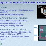
I have participated to a panel during IP-SoC, I must say that “Subsystem IP, myth or Reality” was a great moment. The panel was a mix of mid-size IP vendor (CAST, Sonics), one large EDA (Martin Lund from Cadence), Semiwiki blogger and one large IDM (Peter Hirt from STM) who has very well represented the customer side. And, to make the… Read More
Electronic Design Automation
Yield Analysis and Diagnosis Webinar
Sign up for a free webinar on December 11 on Accelerating Yield and Failure Analysis with Diagnosis.
The one hour presentation will be delivered via webcast by Geir Eide, Mentor’s foremost expert in yield learning. He will cover scan diagnosis, a software-based technique, that effectively identifies defects in digital logic… Read More
Apache Power Artist Capabilities I
I sat down last week with Paul Traynar who was over from UK. He is Apache’s PowerArtist guru. The first thing we talked about was PowerArtist’s sequential power reduction capabilities.
Forward propagation of enables means that when a register is clock gated and feeds a downstream register then that register can be… Read More
A Brief History of the Fabless Semiconductor Ecosystem
Clearly the fabless semiconductor ecosystem is driving the semiconductor industry and is responsible for both the majority of the innovation and the sharp decline in consumer electronics costs we have experienced. By definition, a fabless semiconductor company does not have to spend the time and money on manufacturing related… Read More
Microprocessor Test and Verification 2012
Next week December 10-12th is the Microprocessor Test and Verification (MTV 2012) which is in Austin Texas (as DAC will be next year, of course). After lunch on Monday there is a panel session on the effectiveness of virtual prototyping entitled When simulation suffices, who needs FPGA or emulation? Bill Neifert, the CTO of Carbon… Read More
Formal Analysis of Security Data Paths
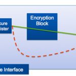
One challenge with security in systems is to ensure that there are not backdoors, either accidentally or maliciously inserted. Intel, ARM and others have various forms of trusted execution technology. Under the hood these are implemented by dividing the design into two parts, normal and secure, and implementing them with physical… Read More
Double Patterning Exposed!
Wanna become the double patterning guru at your company? David Abercrombie, DFM Program Manager for Calibre, has written a series of articles detailing the multifaceted impacts of double patterning on advanced node design and verification. For designers struggling to understand the complexity and nuances of double patterning,… Read More
SystemC vs C++ for High Level Synthesis
One of the decisions that needs to be made when using high-level synthesis (HLS) in general and Catapult in particular is what language to use as input. The choice is C++ or SystemC. Of course at some level SystemC is C++ with added libraries and templates, but in fact the semantics of the two languages end up being very different.
The… Read More
An FPGA Design Flow with Aldec Tools
I’ve used FPGA vendor-supplied tools from both Xilinxand Lattice Semibefore, so I wanted to see what EDA tools Aldec has to offer for FPGA design. I read the Aldecwhite paper, Corporate Standardization of FPGA Design Flow, and summarize what I found.… Read More
Mixed-Signal Methodology Guide: Design Management
I reviewed the book Mixed-Signal Methodology Guidein August of this year published by Cadence, and decided to follow up with one of the authors, Michael Henrie from ClioSoft, to learn more about the importance of Design Management for AMS. Michael is a Software Engineering Manager at ClioSoft and has worked at Zarlink Semi, Legerity,… Read More




Musk’s Orbital Compute Vision: TERAFAB and the End of the Terrestrial Data Center