You are currently viewing SemiWiki as a guest which gives you limited access to the site. To view blog comments and experience other SemiWiki features you must be a registered member. Registration is fast, simple, and absolutely free so please,
join our community today!
            WP_Term Object
(
    [term_id] => 159
    [name] => Siemens EDA
    [slug] => siemens-eda
    [term_group] => 0
    [term_taxonomy_id] => 159
    [taxonomy] => category
    [description] =>
    [parent] => 157
    [count] => 841
    [filter] => raw
    [cat_ID] => 159
    [category_count] => 841
    [category_description] =>
    [cat_name] => Siemens EDA
    [category_nicename] => siemens-eda
    [category_parent] => 157
    [is_post] =>
)

WP_Term Object
(
    [term_id] => 159
    [name] => Siemens EDA
    [slug] => siemens-eda
    [term_group] => 0
    [term_taxonomy_id] => 159
    [taxonomy] => category
    [description] =>
    [parent] => 157
    [count] => 841
    [filter] => raw
    [cat_ID] => 159
    [category_count] => 841
    [category_description] =>
    [cat_name] => Siemens EDA
    [category_nicename] => siemens-eda
    [category_parent] => 157
    [is_post] =>
)
Daniel is joined by Sagar Saxena, Senior Product Engineer at Siemens EDA specializing in computational lithography, optical proximity correction (OPC), and advanced patterning solutions for leading-edge semiconductor manufacturing. Sagar has led the development and deployment of advanced OPC technologies, including… Read More
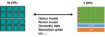
As systems become increasingly complex across every field of science and engineering, the importance of computer simulation in design, analysis, and verification continues to increase over time. The traditional process in which a system is modeled and simulated in a single tool is called monolithic simulation. On the other… Read More
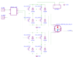
As semiconductor manufacturing pushes toward advanced nodes with tighter feature sizes, the optical proximity correction (OPC) workflow is adopting curvilinear masks to achieve the larger process windows that traditional Manhattan geometries cannot deliver.
Traditional Manhattan masks constrain shapes to vertical … Read More
The semiconductor industry is entering a transformative new phase, driven by the convergence of artificial intelligence, cloud computing, and increasingly complex chip architectures. That message took center stage during the keynote talks at the Siemens EDA User2User 2026 North America conference. Executives from Siemens,… Read More
The semiconductor industry creates increasingly complex SoC and chiplets using lots of IP and all of that IP needs to be characterized at the cell level. As we design with 3nm and 2nm nodes, the sheer volume of data required for accurate static timing analysis (STA) is greatly increasing. Modern design flows rely on characterized… Read More
I was born in the UK (then still a part of Europe), so always eager to see them succeed. But I must admit that past behavior has reinforced the view that the EU’s only active “contribution” to progress is regulation. However this seems to be changing in multiple interesting ways. On a grand scale, the Nordic economic model is taking … Read More
At the recent TSMC Technology Symposium 2026, Siemens EDA reinforced its position as one of the key ecosystem partners supporting TSMC in the race toward AI-driven semiconductor design, advanced packaging, and next-generation process technologies. The annual forum has become one of the semiconductor industry’s most important… Read More
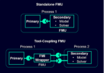
Co-simulation, two or more simulations running concurrently in some manner, is not a new idea. I have written before about multiphysics systems able to model thermal, stress, CFD and other factors simultaneously. I just read a white paper from Siemens based on a different method, using an open standard called the Functional Mockup… Read More
Given the success of the event in Silicon Valley last week, I would expect the Siemens U2U event in Munich to be even bigger. In my experience this has been the best user driven event in 2026 with the deepest customer content. EDA has always been a customer driven industry and it is good to see us recognize that from time to time. Kalar … Read More
By Samar Abd El-Hady and Wael ElManhawy
Design teams today face an uncomfortable truth: the specialized tools they need to verify modern ICs can’t reliably share the same design data. As geometries shrink below five nanometers and designs incorporate billions of transistors across multiple dies, no single Electronic… Read More