You are currently viewing SemiWiki as a guest which gives you limited access to the site. To view blog comments and experience other SemiWiki features you must be a registered member. Registration is fast, simple, and absolutely free so please,
join our community today!
            WP_Term Object
(
    [term_id] => 18712
    [name] => Keysight EDA
    [slug] => keysight-eda
    [term_group] => 0
    [term_taxonomy_id] => 18712
    [taxonomy] => category
    [description] =>
    [parent] => 157
    [count] => 49
    [filter] => raw
    [cat_ID] => 18712
    [category_count] => 49
    [category_description] =>
    [cat_name] => Keysight EDA
    [category_nicename] => keysight-eda
    [category_parent] => 157
    [is_post] =>
)

WP_Term Object
(
    [term_id] => 18712
    [name] => Keysight EDA
    [slug] => keysight-eda
    [term_group] => 0
    [term_taxonomy_id] => 18712
    [taxonomy] => category
    [description] =>
    [parent] => 157
    [count] => 49
    [filter] => raw
    [cat_ID] => 18712
    [category_count] => 49
    [category_description] =>
    [cat_name] => Keysight EDA
    [category_nicename] => keysight-eda
    [category_parent] => 157
    [is_post] =>
)
Back in the late 1990s, Sente launched a product called WattWatcher to estimate power from design RTL and simulation activity. This was revolutionary for its time since alternatives, while very accurate, only offered power analysis at the gate level. Gate-level analysis is great for fine-tuning power but is unhelpful for achieving… Read More
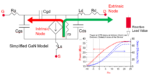
Load-pull power amplifier (PA) design techniques determine the optimal impedances at the power transistor’s extrinsic reference plane, which is the physically accessible boundary for measurement or simulation. This reference plane can be the package transistor leads, die bond pads, or IC chip terminals. It includes… Read More
At lower frequencies with simpler modulation, RF power amplifier (PA) designers could safely concentrate on a few primary metrics – like gain and bandwidth – and rely on relaxed margins to ensure proper operation in a range of conditions. Today’s advanced RF PA design is a different story. mmWave and sub-THz frequencies introduce… Read More
High-speed digital (HSD) design is one of the more exciting areas in EDA right now, with design practices, tools, and workflows evolving to keep pace with increasing design complexity. With the annual Chiplet Summit and DesignCon festivities right around the corner, we sat down with Keysight’s Hee-Soo Lee, HSD Segment Lead, … Read More
Tell us a little bit about yourself and your company.
I’m Nilesh Kamdar, General Manager of the Keysight EDA business unit. Keysight is an S&P 500 company that provides design, emulation, and test solutions to help engineers develop and deploy faster with less risk. On the EDA side, we focus on RFMW, high-speed digital,… Read More
In the fast-evolving world of electronic design automation (EDA), where complexity multiplies with every nanometer shrink and AI integration, data silos are the silent killers of innovation. Keysight Technologies, a leader in design and test solutions, tackles this head-on with their webinar “From Silos to Systems,… Read More
Given my physics background I’m ashamed to admit I know very little about quantum computers (QC) though I’m now working to correct that defect. Like many of you I wanted to start with the basics: what are the components and systems in the physical implementation of a quantum “CPU” and how do they map to classical CPUs? I’m finding the… Read More
Daniel is joined by Pedro Pires, a product and technology leader with a strong background in IP and data management within the EDA industry. Currently a product manager at Keysight Technologies, he drives the roadmap for the AI-driven data management solutions. Pedro’s career spans roles in software engineering and data science… Read More
In this episode of the Semiconductor Insiders video series, Dan is joined by Mohamed Hassan, who leads the Quantum EDA segment at Keysight. Mohamed provides a broad overview of superconducting quantum system design. He discusses the challenges for this design style and how EDA requirements for quantum design differ from
…
Read More
Why should high frequency circuit designers consider stability early in the design process? Isn’t there enough to worry about just making the circuit function at the fundamental frequency?
In the past, Microwave Engineers used to solve stability problems in the lab, perhaps adding bypassing or loss in a strategic location to… Read More