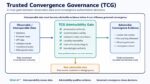
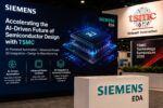
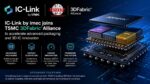
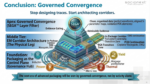
BannerforSemiWiki 800x100 (2)
WP_Term Object
(
    [term_id] => 19172
    [name] => Chiplet
    [slug] => chiplet
    [term_group] => 0
    [term_taxonomy_id] => 19172
    [taxonomy] => category
    [description] => 
    [parent] => 0
    [count] => 170
    [filter] => raw
    [cat_ID] => 19172
    [category_count] => 170
    [category_description] => 
    [cat_name] => Chiplet
    [category_nicename] => chiplet
    [category_parent] => 0
    [is_post] => 
)

Revolutionizing Chip Packaging: The Impact of Intel’s Embedded Multi-Die Interconnect Bridge (EMIB)

Revolutionizing Chip Packaging: The Impact of Intel’s Embedded Multi-Die Interconnect Bridge (EMIB)
by Admin on 08-27-2025 at 10:00 am

Intel Foundry Packaging Evolution 2025

In an era dominated by artificial intelligence (AI), machine learning (ML), and high-performance computing (HPC), the demand for semiconductors that deliver high data throughput, low latency, and energy efficiency has never been greater. Traditional chip designs often struggle to keep pace with these requirements, leading… Read More


Breaking out of the ivory tower: 3D IC thermal analysis for all

Breaking out of the ivory tower: 3D IC thermal analysis for all
by Admin on 08-26-2025 at 6:00 am

figure 1

Todd Burkholder and Andras Vass-Varnai, Siemens EDA

As semiconductor devices become smaller, more powerful and more densely integrated, thermal management has shifted from an afterthought to a central challenge in modern IC design. In contemporary 3D IC architectures—where multiple chiplets are stacked and closely arrayed—power… Read More


Chiplets: providing commercially valuable patent protection for modular products

Chiplets: providing commercially valuable patent protection for modular products
by Robbie Berryman on 08-24-2025 at 6:00 am

Screenshot 2025 07 27 at 08 32 09

Many products are assembled from components manufactured and distributed separately, and it is important to consider how such products are manufactured when seeking to provide commercially valuable patent protection. This article provides an example in the field of computer chip manufacture.

Chiplets

A system-on-a-chip

Read More

Streamlining Functional Verification for Multi-Die and Chiplet Designs

Streamlining Functional Verification for Multi-Die and Chiplet Designs
by Daniel Nenni on 08-14-2025 at 6:00 am

Streamlining Functional Verification for Multi Die and Chiplet Designs

As multi-die and chiplet-based system designs become more prevalent in advanced electronics, much of the focus has been on physical design challenges. However, verification—particularly functional correctness and interoperability of inter-die connections—is just as critical. Interfaces such as UCIe or custom interconnects… Read More


UCIe 3.0: Doubling Bandwidth and Deepening Manageability for the Chiplet Era

UCIe 3.0: Doubling Bandwidth and Deepening Manageability for the Chiplet Era
by Daniel Nenni on 08-05-2025 at 10:00 am

Chiplet SemiWiki UCIe

The Universal Chiplet Interconnect Express (UCIe) 3.0 specification marks a decisive step in the industry’s shift from monolithic SoCs to modular, multi-die systems. Released on August 5, 2025, the new standard doubles peak link speed from 32 GT/s in UCIe 2.0 to 48 and 64 GT/s while adding a suite of manageability and efficiency

Read More

CoPoS is a Bigger Canvas for Chiplets and HBM

CoPoS is a Bigger Canvas for Chiplets and HBM
by Admin on 08-03-2025 at 10:00 am

Chip on Panel on Substrate, often shortened to CoPoS, extends the familiar idea of chip on carrier packaging by moving the redistribution and interposer style structures from circular wafers to large rectangular panels. The finished panel assembly is then mounted on an organic or glass package substrate. This shift from round

Read More

AI-Driven Chip Design: Navigating the Future

AI-Driven Chip Design: Navigating the Future
by Admin on 08-02-2025 at 1:00 pm

DAC 62 Systems on Chips

On July 9, 2025, a DACtv session by Dr. Peter Levin explored the transformative impact of artificial intelligence (AI) on chip design, as presented in the YouTube video. The speaker, an industry expert, delved into how AI is reshaping electronic design automation (EDA), addressing the escalating complexity of modern chips and… Read More


From Atoms to Tokens: Semiconductor Supply Chain Evolution

From Atoms to Tokens: Semiconductor Supply Chain Evolution
by Admin on 08-02-2025 at 7:00 am

On July 18, 2025, a DACtv session titled “From Atoms to Tokens” explored the semiconductor supply chain’s transformation, as presented in the YouTube video. The speaker tackled the challenges and innovations from the atomic level of chip fabrication to the tokenized ecosystems of AI-driven data centers, emphasizing the critical… Read More


Enabling the Ecosystem for True Heterogeneous 3D IC Designs

Enabling the Ecosystem for True Heterogeneous 3D IC Designs
by Kalar Rajendiran on 07-28-2025 at 10:00 am

The Shift to System Technology Co Optimization

The demand for higher performance, greater configurability, and more cost-effective solutions is pushing the industry toward heterogeneous integration and 3D integrated circuits (3D ICs). These solutions are no longer reserved for niche applications—they are rapidly becoming essential to mainstream semiconductor design.… Read More


Alphawave Semi and the AI Era: A Technology Leadership Overview

Alphawave Semi and the AI Era: A Technology Leadership Overview
by Daniel Nenni on 07-14-2025 at 8:00 am

AI Market Silicon Forecast 2025

The explosion of artificial intelligence (AI) is transforming the data center landscape, pushing the boundaries of compute, connectivity, and memory technologies. The exponential growth in AI workloads—training large language models (LLMs), deploying real-time inference, and scaling distributed applications—has … Read More