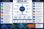
Epitaxial stacks of silicon and silicon germanium are emerging as a key materials platform for three dimensional dynamic random access memory. Future DRAM will likely migrate from vertical channels to horizontally stacked channels that resemble the gate all around concept in logic. That shift demands a starter material made… Read More
Synopsys Webinar – Enabling Multi-Die Design with Intel
As we all know, the age of multi-die design has arrived. And along with it many new design challenges. There is a lot of material discussing the obstacles to achieve more mainstream access to this design architecture, and some good strategies to conquer those obstacles. Synopsys recently published a webinar that took this discussion… Read More
CoPoS is a Bigger Canvas for Chiplets and HBM
AI-Driven Verification: Transforming Semiconductor Design
In a DACtv session on July 9, 2025, Abhi Kolpekwar, Vice-President & General Manager at Siemens EDA, illuminated the transformative role of artificial intelligence (AI) in addressing the escalating challenges of semiconductor design verification. The presentation underscored the limitations of traditional methods… Read More
cHBM for AI: Capabilities, Challenges, and Opportunities
AI’s exponential growth is transforming semiconductor design—and memory is now as critical as compute. Multi-die architecture has emerged as the new frontier, and custom High Bandwidth Memory (cHBM) is fast becoming a cornerstone in this evolution. In a panel session at the Synopsys Executive Forum, leaders from AWS, Marvell,… Read More
Enabling the Ecosystem for True Heterogeneous 3D IC Designs
The demand for higher performance, greater configurability, and more cost-effective solutions is pushing the industry toward heterogeneous integration and 3D integrated circuits (3D ICs). These solutions are no longer reserved for niche applications—they are rapidly becoming essential to mainstream semiconductor design.… Read More
Scaling 3D IC Technologies – Siemens Hosts a Meeting of the Minds at DAC
3D IC was a very popular topic at DAC. The era of heterogeneous, multi-chip design is here. There were a lot of research results and practical examples presented. What stood out for me was a panel at the end of day two of DAC that was hosted by Siemens. This panel brought together an impressive group of experts to weigh in on what was really… Read More
Alchip Launches 2nm Design Platform for HPC and AI ASICs, Eyes TSMC N2 and A16 Roadmap
Alchip Technologies, a global leader in high-performance computing (HPC) and AI infrastructure ASICs, has officially launched its 2nm Design Platform, marking a major advancement in custom silicon design. The company has already received its first 2nm wafers and is collaborating with customers on the development of high-performance… Read More
Altair SimLab: Tackling 3D IC Multiphysics Challenges for Scalable ECAD Modeling
The semiconductor industry is rapidly moving beyond traditional 2D packaging, embracing technologies such as 3D integrated circuits (3D ICs) and 2.5D advanced packaging. These approaches combine heterogeneous chiplets, silicon interposers, and complex multi-layer routing to achieve higher performance and integration.… Read More
Dual Strategy of Electroless Metal Deposition and Surface Silylation Toward Scalable Low-Temperature Hybrid Bonding for Advanced Packaging Applications
In extreme ultraviolet lithography (EUVL) systems, the collector mirror is a critical optical component that gathers and directs EUV light from the source toward the projection optics. Over time, the collector surface accumulates contaminant films — primarily tin (Sn) debris from the laser-produced plasma (LPP) source, … Read More
Rapidus, IBM, and the Billion-Dollar Silicon Sovereignty Bet