
The recent Chiplet Summit 2026 was a great place to learn about new chiplet designs, emerging standards, and a growing array of support technologies to help design and manufacture chiplet-based systems. In my travels at the show, I found a lot of technology that fit these descriptions. But there were also companies at the show that… Read More

Author: Mike Gianfagna
proteanTecs at Chiplet Summit – Changing the Game for Health & Performance Monitoring of Chiplets

Analog Bits Demos Real-Time On-Chip Power Sensing and Delivery on N2P at the TSMC 2026 Technology Symposium
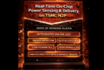
Analog Bits has a way of stealing the show at every event they attend. The formula is actually quite straight-forward – come to the show with the most relevant, highest impact IP running on the most advanced process. The company will be applying this strategy again at the upcoming TSMC 2026 Technology Symposium with an array of real-time… Read More
Exploring the Hidden Complexity of Modern Power Electronics Design – A Siemens White Paper
Review the specifications of any state-of-the-art microcontroller and you will discover the high dynamic current the device can consume. Examining the high clock rates and low tolerable voltage drop will lead you to the all-important power delivery network, or PDN. Components here include power planes, layer stack-up, decoupling… Read More
yieldHUB Expands Its Impact with New Technology and a New Website

yieldHUB is a unique company that focuses on yield optimization for the semiconductor industry. The company aims to bring engineering teams together with a platform that allows sharing of data analytics and knowledge about products to improve yield. This goal is certainly fueled by unifying data from multiple steps in the manufacturing… Read More
yieldWerx Delivers a Master Class in Co-Packaged Photonics Implementation
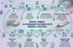
We all know the semiconductor industry is seeing a new era of data intensity. The industry’s response includes advanced semiconductor design strategies, the adoption of chiplets, and the integration of optical I/O and photonics to enable higher performance, faster AI computation, and increased modularity. Co-packaged photonics… Read More
Samtec’s Strong Presence at embedded world 2026
The embedded world Exhibition & Conference recently concluded. The event is held annually in Nuremberg, Germany and has become one of the most influential gatherings for the global embedded systems community. Since its inception in 2003, the event has grown from a modest technical meeting into a large-scale international… Read More
Webinar – How to Reclaim Margin in Advanced Nodes

This informative webinar discusses a significant issue that is cropping up for sub-5nm designs. As the graphic above shows, modeling uncertainty at advanced nodes results in excessive guard banding. These guard bands result in reduced performance and profit. A loss of 25 – 35% in PPA is discussed, along with the lost profit associated… Read More
Arteris Highlights a Path to Scalable Multi-Die Systems at the Chiplet Summit

At the recent Chiplet Summit, presentations, discussions and general participation could be broken down into a few broad categories. There were presentations of actual chiplet designs, either as building blocks or end products. There were presentations regarding design tools and methodologies to support and accelerate … Read More
Siemens Wins Best in Show Award at Chiplet Summit and Targets Broad 3D IC Design Enablement

The recent Chiplet Summit in Santa Clara was buzzing with new designs and new design methods. It felt like the industry had turned a corner at this year’s event with lots of new technology and design success on display. Siemens EDA had a large presence at the show and took home the Best in Show Award for Packaging Design. There were a … Read More
Synopsys Explores AI/ML Impact on Mask Synthesis at SPIE 2026

The SPIE Advanced Lithography + Patterning Symposium recently concluded. This is a popular event where leading researchers gather. Challenges such as optical and EUV lithography, patterning technologies, metrology, and process integration for semiconductor manufacturing and adjacent applications are all covered. This… Read More


Why Huawei Says It Will Match TSMC’s Most Advanced Chips by 2031