
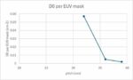
Earlier this month, TechInsights did a teardown of the Kirin 9030 chip found in Huawei’s Mate 80 Pro Max [1]. Two clear statements were made on the findings: (1) the transistor density of SMIC’s “N+3” process was definitely below that of the earlier 5nm processes from Samsung and TSMC, and (2) metal pitch was aggressively scaled

Author: Fred Chen
Kirin 9030 Hints at SMIC’s Possible Paths Toward >300 MTr/mm2 Without EUV
Self-Aligned Spacer Patterning for Minimum Pitch Metal in DRAM

The patterning of features outside a DRAM cell array can be just as challenging as those within the array itself [1]. The array contains features which are densely packed, but regularly arranged. On the other hand, outside the array, the minimum pitch features, such as the lowest metal lines in the periphery for the sense amplifier… Read More
Via Multipatterning Regardless of Wavelength as High-NA EUV Lithography Becomes Too Stochastic
For the so-called “2nm” node or beyond, the minimum metal pitch is expected to be 20 nm or even less, while at the same time, contacted gate pitch is being pushed to 40 nm [1]. Therefore, we expect via connections that can possibly be as narrow as 10 nm (Figure 1)! For this reason, it is natural to expect High-NA EUV lithography as the go-to
EUV Lithography Without Pellicles: Accounting for Low Yields
While stochastic defects link yield with the practical resolution of EUV lithography resulting from its quantum nature [1], very low yields of EUV processes are more readily linked to the use of EUV masks without pellicles. Pellicles are thin film membrane covers on masks (regardless of wavelength: EUV and DUV and i-line) used… Read More
EUV Resist Degradation with Outgassing at Higher Doses
Dosing for EUV lithography walks a fine line between productivity and defectivity. Fabs can choose higher-dose exposures to suppress photon shot noise [1]. However, higher doses require EUV machines to scan the wafer at slower speeds, degrading throughput [2].
On the other hand, there is the threat of resist thickness loss that… Read More
IMEC’s Advanced Node Yield Model Now Addresses EUV Stochastics
It lays the foundation for the Stochastics Resolution Gap
Chris Mack, the CTO of Fractilia, recently wrote of the “Stochastics Resolution Gap,” which is effectively limiting the manufacturability of EUV despite its ability to reach resolution limits approaching 10 nm in the lab [1,2]. As researchers have inevitably found, … Read More
Facing the Quantum Nature of EUV Lithography
The topics of stochastics and blur in EUV lithography has been examined by myself for quite some time now [1,2], but I am happy to see that others are pursuing this direction seriously as well [3]. As advanced node half-pitch dimensions approach 10 nm and smaller, the size of molecules in the resist becomes impossible to ignore for… Read More
High-NA Hard Sell: EUV Multi-patterning Practices Revealed, Depth of Focus Not Mentioned
In High-NA EUV lithography systems, the numerical aperture (NA) is expanded from 0.33 to 0.55. This change has been marketed as allowing multi-patterning on the 0.33 NA EUV systems to be avoided. Only very recently have specific examples of this been provided [1]. In fact, it can be shown that double patterning has been implemented… Read More
Impact of Varying Electron Blur and Yield on Stochastic Fluctuations in EUV Resist
A comprehensive update to the EUV stochastic image model
In extreme ultraviolet (EUV) lithography, photoelectron/secondary electron blur and secondary electron yield are known to drive stochastic fluctuations in the resist [1-3], leading to the formation of random defects and the degradation of pattern fidelity at advanced
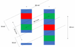
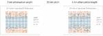
Stitched Multi-Patterning for Minimum Pitch Metal in DRAM Periphery
In a DRAM chip, the memory array contains features which are the most densely packed, but at least they are regularly arranged. Outside the array, the regularity is lost, but in the most difficult cases, the pitches can still be comparable with those within the array, though generally larger. Such features include the lowest metal… Read More


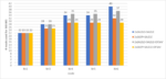
The Memory Sector Is Becoming One of the Main Beneficiaries of the AI Boom