

VSORA AI Processor Raises $46 Million to Fast-Track Silicon Development
We stand on the cusp of an era defined by ubiquitous intelligence—a stone’s throw from a tidal wave of AI-powered products underpinned by next-generation silicon. Realizing that future demands nothing less than a fundamental rethink of how we design semiconductors and architect computers.
At the core of this transformation is a simple—but profound—shift: AI silicon must be shaped by AI workloads from day one. Gone are the days when hardware and software evolve in parallel—and only converge at validation, by which point the architecture is set in stone. Today’s paradigm demands re-engineer engineering, i.e., software-defined hardware design, tightly integrating AI code and silicon from the ground up.
Brute Force, No Grace: GPUs Hit the Memory Wall Processing LLMs
Today, the dominant computing architecture for AI processors is the Graphics Processing Unit (GPU). Originally conceived in 1999, when Nvidia released the GeForce 256 marketed as the “world’s first GPU”, it addressed the growing demand for parallel processing in rendering computer graphics. The GPU has since been repurposed to handle the massive, highly parallel workloads required by today’s AI algorithms—particularly those based on large language models (LLMs).
Despite significant advancements in GPU theoretical throughput, GPUs still face fundamental limitations, namely, poor computational efficiency, high power consumption, and suboptimal latency. To exemplify, a GPU with a theoretical peak performance of one PetaFLOPS and a realistic efficiency of 10% when processing a state-of-the-art LLM such as GPT-4 or LLM3-405B (noting that efficiency varies depending on the specific algorithm), would in practice deliver only 100 TeraFLOPS. To achieve a sustained PetaFLOPS of performance, 10 such GPUs would be required resulting in substantial more power consumption than that of a single device. Less apparent, this configuration also introduces significantly longer latency, compounding the inefficiencies.
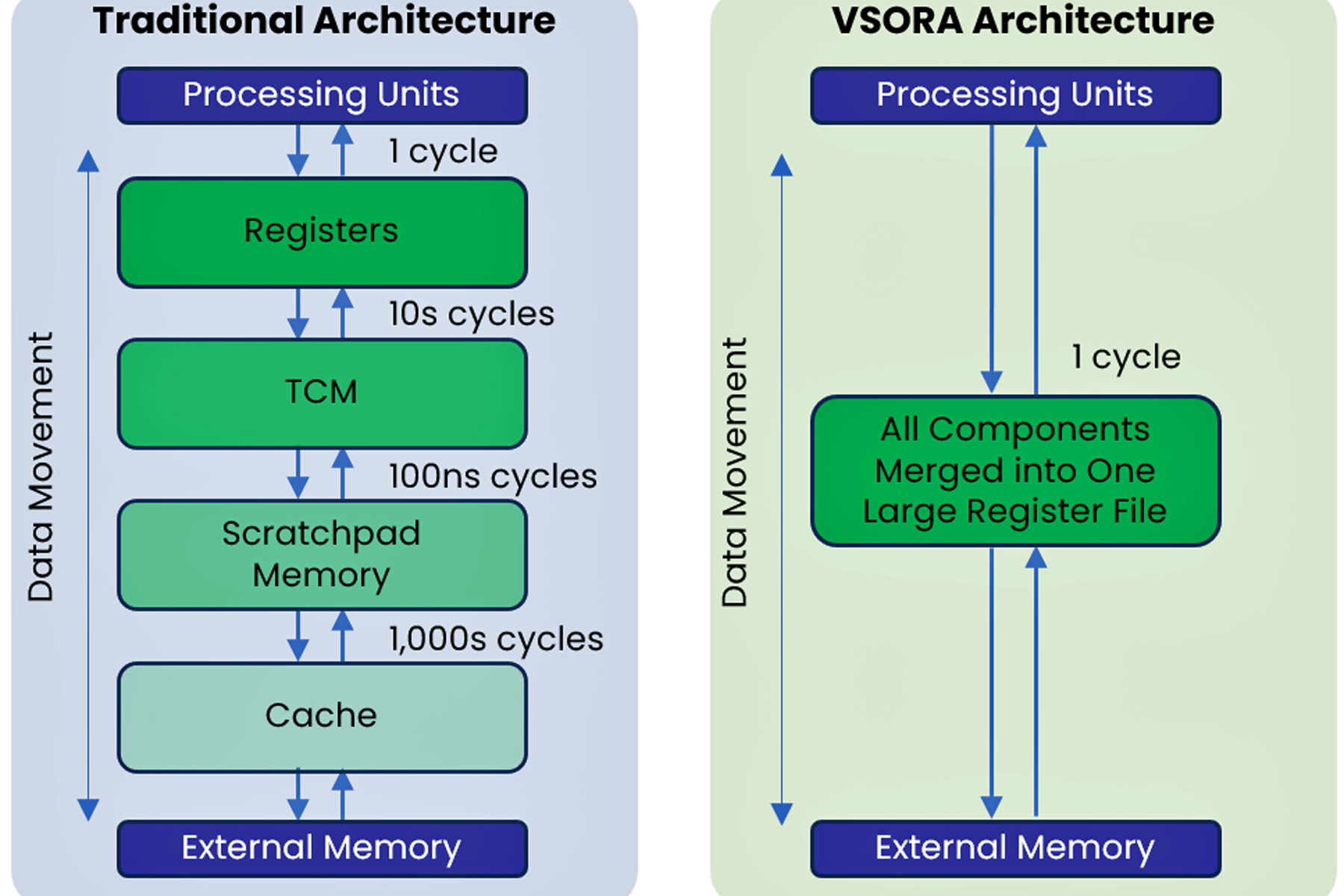
Peeling back the layers of a GPU would uncover the culprit behind its poor efficiency: the memory wall. This long-standing bottleneck arises from an ever-widening gap between the insatiable demand of compute cores for data and the finite bandwidth of off-chip memory. As a result, cores frequently stall waiting on data transfers, preventing sustained utilization even when computational resources are plentiful.
Enhancements to the memory bandwidth via layered access in the form of multi-level caches have helped mitigate the impact—until the advent of AI workloads exposed this limitation. GPU’s brute-force approach, necessary to handle large language models (LLM), comes at a price: poor efficiency resulting in high energy consumption and long latency.
While GPU limitations during LLM training primarily manifest as increased computational cost, they pose a more critical obstacle during inference. This is especially pronounced in edge deployments, where stringent power budgets and real-time latency requirements, crucial for applications like autonomous driving, severely restrict GPU viability.
The VSORA Solution: Knocking Down the Memory Wall
While the semiconductor industry is intensely focused on mitigating the memory bandwidth bottleneck that plagues LLM inference processing, French startup VSORA has quietly pioneered a disruptive solution. The solution represents a paradigm shift in memory management.
VSORA Architecture: Functional Principles
The VSORA’s architecture redefines how data is stored, moved, and processed at scale. At its heart lies an innovative scalable compute core designed around a very fast tightly-coupled-memory (TCM).
The TCM functions like an expansive and vast register file—offering the lowest-latency, single-cycle read/write access of any on-chip memory. Placed directly alongside the compute fabric, it bypasses the multi-cycle penalties of conventional cache hierarchies. As a result, VSORA maintains exceptionally high utilization even on irregular workloads, since hot data is always available in the very next cycle.
Together, the compute logic and the TCM form a unified, scalable compute core that minimizes data-movement overhead and bypasses traditional cache hierarchies. The result is an order-of-magnitude reduction in access latency and blazing-fast end-to-end inference performance across edge and data-center deployments. See figure 1.

VSORA Architecture: Physical Implementation
The VSORA architecture is realized using a chiplet-based design within a 2.5D silicon‐interposer package, coupling compute chiplets to high-capacity memory chiplets. Each compute chiplet carries two VSORA basic compute cores, and each memory chiplet houses a high-bandwidth memory stack. Compute and memory chiplets communicate over an ultra-low-latency, high-throughput Network-on-Chip (NoC) fabric.
In the flagship Jotunn8 device, eight compute chiplets and eight HBM3e chiplets are tiled around the central interposer, delivering massive aggregate bandwidth and parallelism in a single package.
Beyond Bandwidth/Latency: VSORA’s On-the-Fly Re-configurable Compute Cores Unlock Algorithm-Agnostic Deployment
In most AI accelerators today, the fundamental compute element is a single-bit multiply-accumulate (MAC) unit. Thousands—or even hundreds of thousands—of these MACs are woven together in a massive array, with both the compiler and the user defining how data flows spatially across the array and in what temporal order each operation executes. While this approach excels at raw throughput for uniform, fixed-precision workloads, it begins to fracture under the demands of modern large language models and cutting-edge AI applications, which require:
- Mixed-precision support: LLMs often need to employ different quantization on different layers, for example, a mix of FP8 Tensorcore, FP16 Tensorcore and FP16 DSP layers within the same network to balance performance, accuracy and numerical fidelity. This requires the system to repeatedly quantize and dequantize data, introducing both overhead and rounding error
- Dynamic range management: Activations and weights span widely varying magnitudes. Architectures built around a single bit can struggle to represent very large or very small values without resorting to costly software-driven scaling.
- Irregular and sparse tensors: Advanced workloads increasingly exploit sparsity to prune redundant connections. A rigid MAC mesh, optimized for dense operations, underutilizes its resources when data is sparse or when operations deviate from simple dot products.
These limitations introduce bottlenecks and reduce accuracy, consequently throughput drops when precision conversions don’t map neatly onto the MAC fabric, and critical data must shuffle through auxiliary units for scaling or activation functions.
VSORA’s architecture flips the script on traditional accelerator fabrics by adopting reconfigurable compute tiles that adapt on the fly—zero downtime, zero manual reprogramming. Instead of dedicating large swaths of silicon to fixed-function MAC arrays or rigid tensor cores, each VSORA tile can instantly assume either DSP-style or Tensorcore-style operation, at any precision (FP8, FP16, INT8, etc.), on a per-layer basis.
In practice, this means that:
- Layer-optimal precision: One layer might run at FP16 with high-dynamic-range DSP operations for numerically sensitive tasks, then the very next layer switches to FP8 Tensorcore math for maximum throughput—without any pipeline stalls.
- Resource consolidation: Because every tile can serve multiple roles, there’s no idle silicon stranded when workloads shift in precision or compute type. VSORA sustains peak utilization across the diverse math patterns of modern LLMs.
- Simplified compiler flow: The compiler’s task reduces to choosing the ideal mode per layer—Tensorcore or DSP—instead of wrestling with mapping data to dozens of discrete hardware blocks.
The result is an accelerator that tunes itself continuously to each model’s needs, delivering higher accuracy, lower latency, and superior energy efficiency compared to static, single-purpose designs.
The VSORA’s architecture is not just about raw bandwidth; it’s about intelligent data processing, tailored to the specific demands of each application. This meticulous attention to detail at the core level is what distinguishes VSORA, enabling them to deliver AI inference solutions that are both powerful and efficient.
VSORA’s Secret Weapon: The Intelligent Compiler
Hardware ingenuity is only half the equation. VSORA’s algorithm-agnostic compiler consists of two stages. A front-end graph, hardware-independent compiler, ingests standard model formats (Tensorflow, PyTorch, ONNX, etc.) and optimizes the model via layer fusion, layer re-ordering, weight compilation and scheduling, slicing, tensor layout optimization, execution scheduling and sparsity enabling (data and weights). A back-end, LLVM-based compiler, fully automates the mapping of leading-edge LLMs—such as Llama—onto the VSORA J8.
VSORA’s architecture radically simplifies the deployment of large language models by replacing the tedious, error-prone mapping workflows common in GPU environments with an automated, software-defined memory management layer. Unlike traditional GPU toolchains—where developers must hand-tune data layouts, manage low-level memory transfers, and master platform-specific APIs such as NVIDIA CUDA—VSORA’s compiler handles all of this transparently. As a result, teams can bring LLMs online far more quickly and reliably, even in power-constrained or latency-sensitive applications, without sacrificing performance or requiring deep hardware-level expertise.
The result is a seamless compilation software stack that maximizes chip utilization, simplifies deployment, and unleashes the full performance potential of VSORA’s breakthrough inference platform.
Conclusion
Unlike general-purpose accelerators optimized for training, VSORA conceived an architecture optimized for inference. The specialization reduces latency, boosts real-world responsiveness, and drives down operational costs in scenarios where every millisecond counts—from on-device AI in smart cameras to safety-critical systems in self-driving cars.
Market research forecasts AI inference revenue to double from about $100 billion in 2025 to an estimated $250 billion by 2030—a 15+ percent compound annual growth rate. As enterprises race to deploy real-time AI at scale, VSORA’s efficiency-first approach could redefine cost structures and performance benchmarks across the industry.
On April 27, 2025, VSORA announced a $46 millions investment led by Otium Capital and a prominent French family office, with participation from Omnes Capital, Adélie Capital, and co-financing by the European Innovation Council Fund. In the words of Khaled Maalej, VSORA founder and CEO, “this funding empowers VSORA to tape-out the chip and ramp up production.”
Also Read:
SNUG 2025: A Watershed Moment for EDA – Part 1
SNUG 2025: A Watershed Moment for EDA – Part 2
DVCon 2025: AI and the Future of Verification Take Center Stage
Share this post via:


Solving the EDA tool fragmentation crisis