Webinars are a powerful way for engineers to get updated on EDA and IC design approaches, so I’m sharing what I viewed last month at a Silvaco webinar on TFT and FPD design. You probably are using a TFT LCD display in your TV, monitor, mobile phone, video game system, GPS device or projector. The custom IC design flow offered by Silvaco is shown below for both front-end and back-end tools:
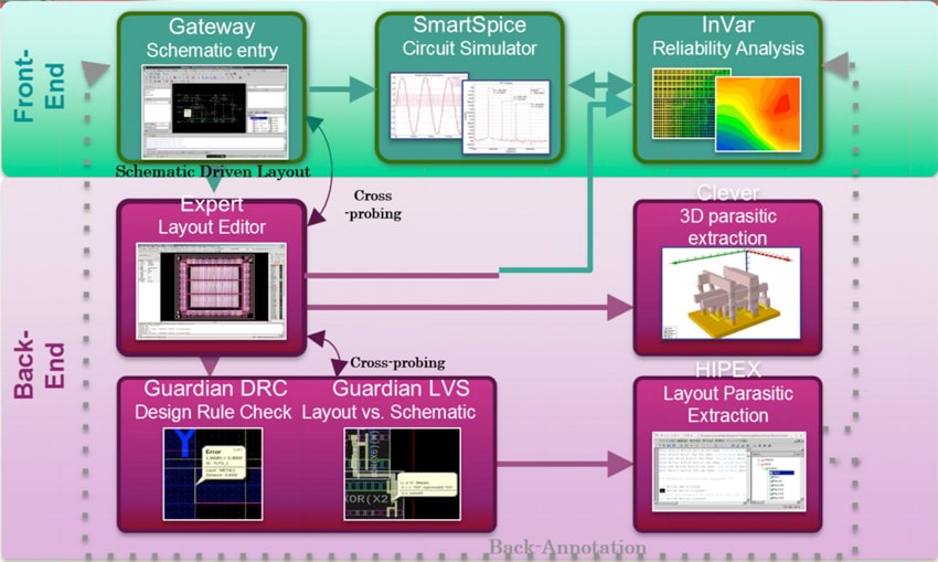
For this webinar they talked about three specific tools used in TFT and FPD design:
- SmartSpice Pro for FastSPICE circuit simulation
- Expert for IC layout editing
- InVar Prime for power integrity analysis
Speaking first was Dr. Gediminas Paulavicius, a senior R&D engineer for the FastSPICE circuit simulator tool called SmartSpice Pro.
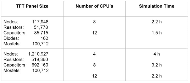
The TFT display panels have millions of active transistors and passive devices along with the challenge of layout dependent effects. If you tried to simulate such a large netlist with a SPICE circuit simulator the capacity would be too large and the run times prohibitive, so a FastSPICE circuit simulator is the best tool for the job. The SmartSpice Pro circuit simulator can handle these large netlists as it does an automatic circuit partitioning, applies event-driven simulation between partitions and matrix-based solvers within each partition along with a specific time-step. Multi-threading is used to help speed up simulation results. Here’s a table showing simulation times versus netlist capacity and the number of CPUs:
Waveforms from SmartSpice Pro are displayed with multiple colors, and circuit designers can verify proper operation and performance by viewing results from transient analysis:
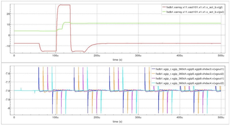
You can expect that the accuracy from this FastSPICE circuit simulator to be within 0.5% of a traditional SPICE circuit simulator.
Related blog – Analyzing All of those IC Parasitic Extraction Results
For the second speaker we heard from Andrei Karabelnikau, Engineering Manager for an IC layout editor called Expert. With the Expert tool you get lots of useful features:
- Hierarchical layout editor
- P-Cell support
- SDL (Schematic Driven Layout)
- Resistance between points
- Real-time DRC
- LVL (Layout Versus Layout)
- Bus commands to route FPD designs with equal resistance routing
- Cross-sectional viewing
- Fast loading of GDSII or OA
Here’s an example of equal resistance routing in Expert:

Technology-specific foundry files are offered in the iPDK format.
Alex Samoylov was the third speaker in this webinar and he showed a power integrity tool called InVar Prime. What makes this tool different from other power integrity tools is that it can be used by a layout engineer early in the design process instead of a circuit design engineer. Here are the inputs required to perform power integrity analysis:
- GDSII layout
- Technology file
- Current source annotation
- Voltage source annotation
A layout engineer can perform several types of analysis with InVar Prime:
- Analysis of planes and signals
- Estimated IR-drop
- Estimated current densities
- Check for missing vias
- Find signal detour routing
- Point to point resistance check
Each one of these analysis steps is performed within the InVar Prime tool, and it doesn’t require a SPICE circuit simulator so the run times are quite short. Here’s what you see for analysis of the distance to voltage sources:
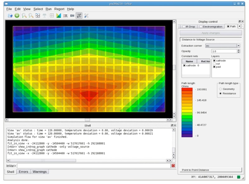
The red region is of concern because the distance to the closest voltage source is too long, so the layout engineer can take steps to improve the layout.
Related blog – Approaches for EM, IR and Thermal Analysis of ICs
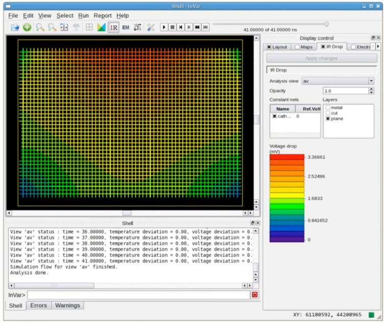
In the next screenshot we can see the results of IR drop analysis across an array, disclosing that we have a layout problem at the very top of the array in the middle, shown in red color:
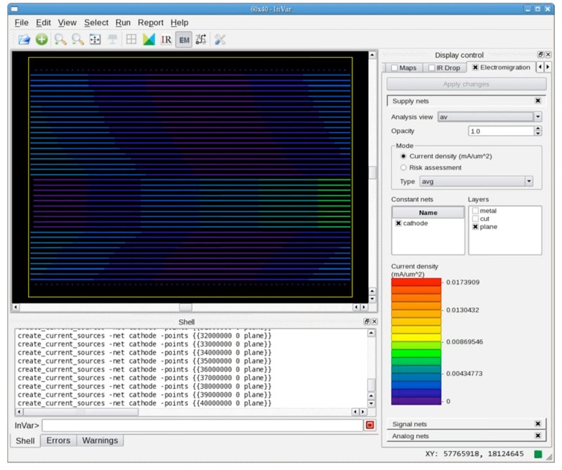
The final type of analysis that was demonstrated shows EM (Electro-Migration) and current density values in rainbow colors where red means an area that should be fixed:
Summary
TFT and FPD designs are characterized as large arrays of transistors that must be accurately analyzed in order to ensure that speed, power, area, current and reliability goals are met. Silvaco has been offering EDA tools in this market segment for years now, and they look to be easy to use, quick to learn, and provide both visual and numerical feedback for custom IC designs.
Silvaco acquired the company Invarian back in 2015 which developed the InVar tool, and it looks like Silvaco will continue to acquire point tool EDA and IP vendors as part of their new growth strategy along with continued internal tool development efforts.
Share this post via:

![SILVACO 051525 Webinar 400x400 v2[62]](https://semiwiki.com/wp-content/uploads/2025/04/SILVACO_051525_Webinar_400x400_v262.jpg)


Comments
There are no comments yet.
You must register or log in to view/post comments.