Back at DAC in 2011 I first started to hear about this EDA company named edXact that specialized in reducing and analyzing IC parasitic extraction results. So Silvaco acquired edXact and I wanted to get an update on what is new with their EDA tools that help help you to analyze and manage the massive amount of extracted RLC and even K values that all impact IC design performance, timing and power. I attended their webinar last week where Jean-Pierre Goujon presented.
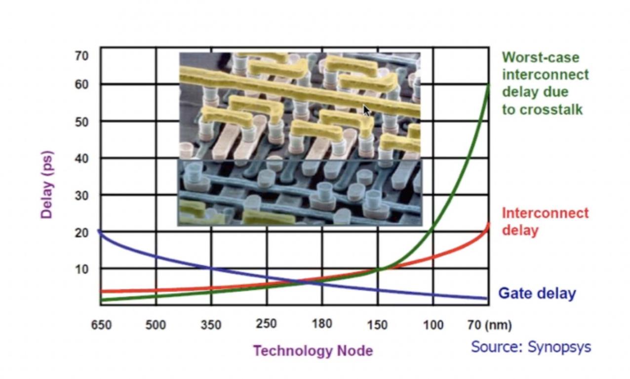
Just take a quick look at the 3D interconnect in the diagram below, and how with each smaller technology node we are seeing interconnect delays rise and the worst-case interconnect delay due to crosstalk dramatically rising:
Related blog – RLCK reduction tool at DAC
The basic idea is that if you can find the sources of these delays then you can do something about it through either cell placement, block placement, routing or transistor sizing. The interconnect in an IC using 60nm technology and smaller are causing more delay than the gates from your cell library. By analyzing your extraction results prior to SPICE simulation you will actually reduce the number of SPICE runs required.
Let’s take a look at the IC design flow for analyzing two slightly different extracted netlists:
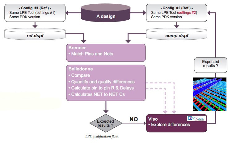
The Viso tool shown in the lower right corner provides design analysis and exploration of parasitics through the following features:
- Viewing resistance and capacitance values, RC time delays
- Analysis in numerical, tabular views
- Graphical views in both 2D and 3D
- Detection of cut nets, dangling nets, sanity checks on DSPF/SPEF/CalibreView
Related blog – CEO Interview: David Dutton of Silvaco
In the middle of the flow is the Belledonne tool, useful for:
- Comparing different extracted netlists (DSPF, SPEF, CalibreView)
- Comparing statistics of: resistance, capacitance, static delays
- Batch or interactive analysis
- PDK optimization and validation
At the top middle is Brenner, an EDA tool that matches pin and net names, so for example if one netlist had an MOS transistor with four fingers named ABCD it could be matched with another netlist where the same four fingers were in a different order, but still equivalent.
Related blog – It’s Time to Put Your SPICE Netlists on a Diet
Live Demo
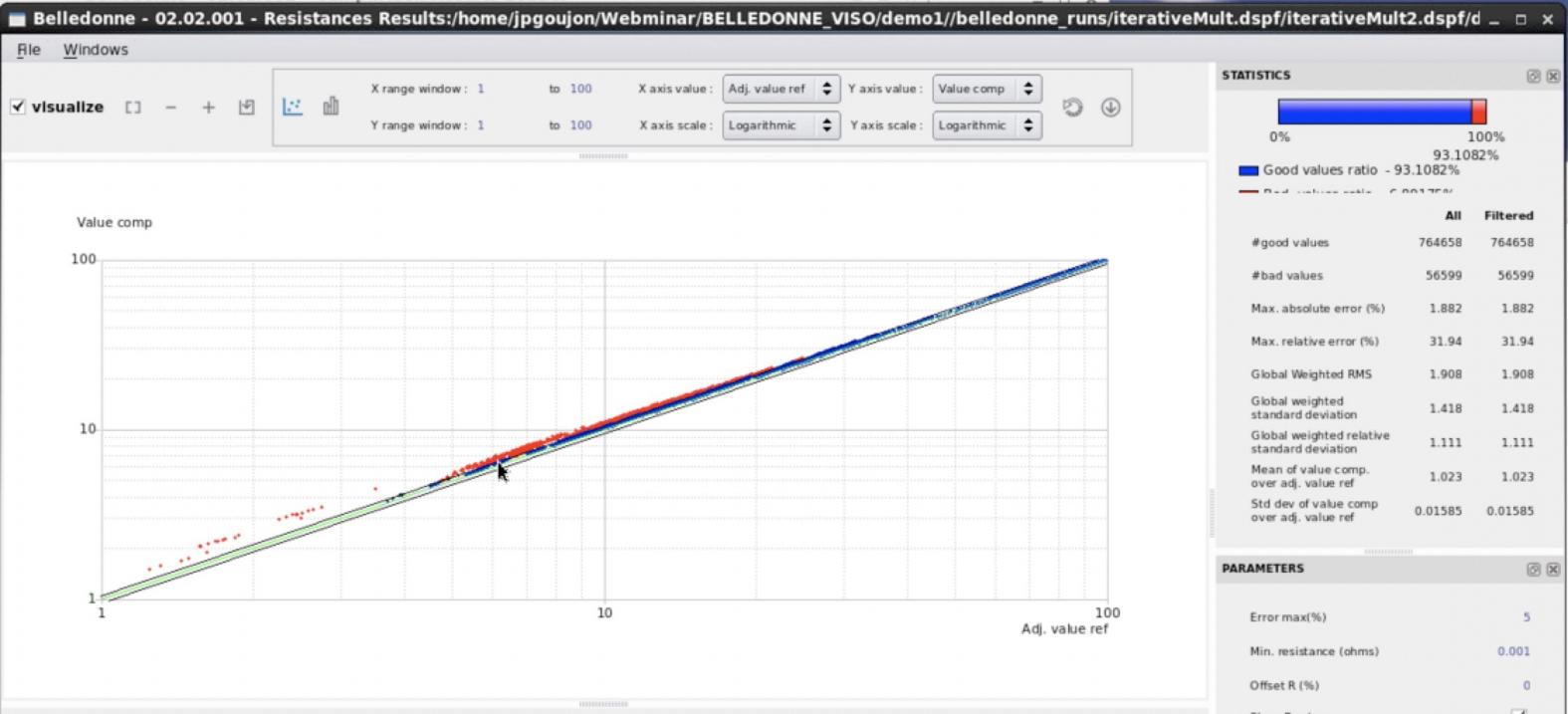
I’m a big believer in showing EDA tools live instead of using canned screen shots, because it actually provides a feeling for how responsive and speedy tools can be. Jean-Pierre started from the Unix command prompt and invoked the GUI called alps, then showed how he uses Belledonne to compare two DSPF files with different pin names. The actual comparison run time for 1 million Resistors was completed in just seconds. Here’s a graphical view comparing resistance values where the color Red depicts over a 5% difference:
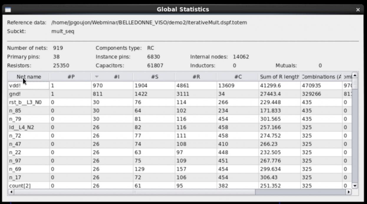
For the second demo circuit we looked at the global statistics from the netlist and then quickly sorted them by maximum RC values shown in a tabular format:
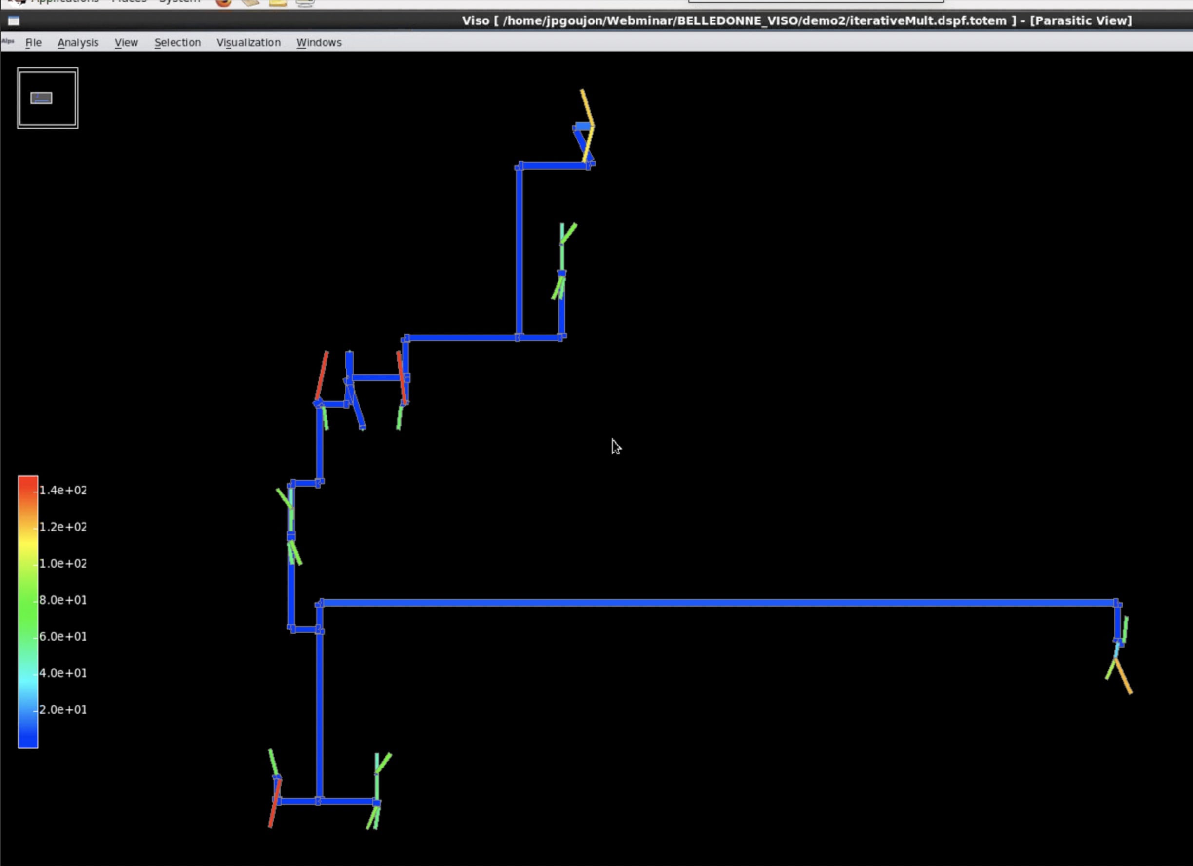
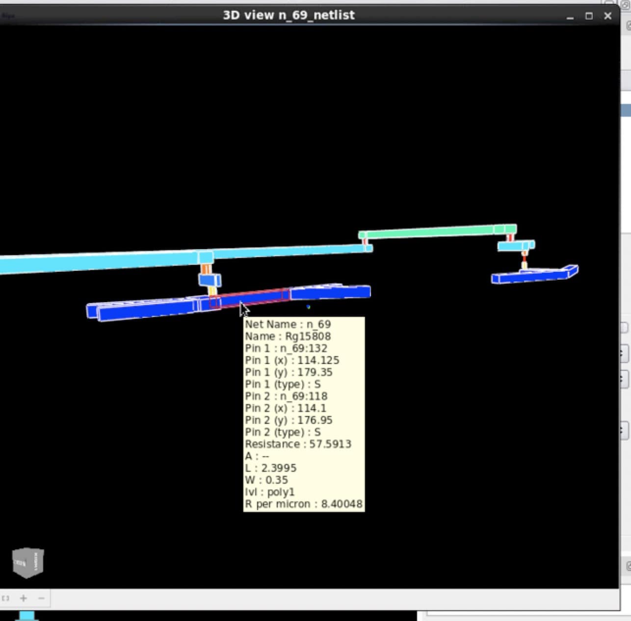
You can click on a particular net and then visualize it in either 2D or 3D views to better understand the physical topology:
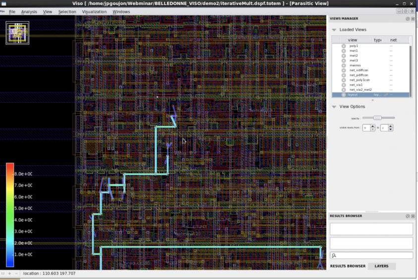
To understand the context of this extracted interconnect you can overlay the results on top of the GDSII layout:
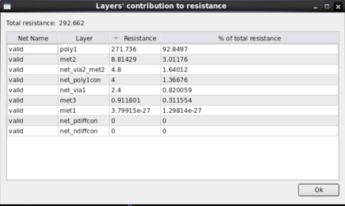
In the third demo we looked at resistance analytics to understand where the maximum pin to pin resistance values were located. Once a high resistance path was found, the layer contribution to resistance was displayed to further pinpoint the greatest contributor. For this selected net it was the poly1 layer contributing to 92% of the total resistance.
2D and 3D results showed resistance values by color to get a quick graphical understanding of where to start looking. We saw pin to pin RC delay values, net to net capacitance tables, and could understand what capacitance with grounded versus coupled.
In the fourth and final demo I got to see how sanity checks could be run to identify opens in the IC layout interconnect caused by missing vias.
Summary
This was very practical webinar where we got to see live EDA tools running that will help IC designers and PDK developers better understand the effects of parasitic RCL values on their particular designs. In the past you may have been tempted to just run extraction and then immediately start running SPICE simulations, however the recommended flow is to perform analysis of the extracted netlists prior to starting SPICE simulation in order to understand and quantify the portions of your design with the most resistance and capacitance values. Circuit designs can now quickly understand where coupling capacitance is impacting their layouts, then decide if they need to make topology changes are go back and start resizing transistors.
The archived webinar is online now here.
Share this post via:

![SILVACO 051525 Webinar 400x400 v2[62]](https://semiwiki.com/wp-content/uploads/2025/04/SILVACO_051525_Webinar_400x400_v262.jpg)


Comments
There are no comments yet.
You must register or log in to view/post comments.