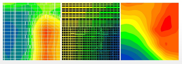
When I designed DRAM chips at Intel back in the 1970’s we didn’t really know what the die temperature would be before taping out silicon, instead we waited for packaged parts to come back and then did our thermal measurements. IC designers today don’t have that luxury of taping out their new SoC without having done some simulations for thermal reliability and power integrity. As an IC is powered up the active transistors start to warm up the local area of the chip, which in turn slows down the timing and reduces the current drive capabilities, so this interdependence needs to be simulated. From a reliability viewpoint the current through the interconnect creates a voltage drop (aka IR drop) and the integrity of the metal interconnect depends on how many amps per square micron that can flow before electromigration effects set in (EM).
I’ve blogged about an EDA vendor named Invarian back in 2013 at DAC when I first learned about their power, thermal, EM and IR tools, then Silvaco acquired Invarian in March 2015. Alex Samoylov from Silvaco spoke with me by phone recently to provide an update on their tools in this area.
Q&A
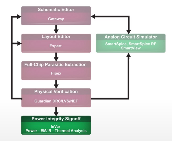
Q: How do your power integrity tools fit into the design flow?
They can be used for standard cell designs at the gate-level, SoC or full-chip level, even at the transistor-level for analog and custom designs.

InVar Design Flow
Q: Is InVar three separate tools?
No, InVar is a bit different than other approaches because it’s a single tool with three types of analysis: Power, EM/IR and Thermal.
Q: Who on the design team would use InVar then?
A layout engineer could start using InVar to help in the routing and planning of the power nets, VDD and VSS. InVar IR will provide them early analysis on how good the power routing is at that point.
On a standard cell approach the design engineer could start with a Verilog netlist and start running power analysis.
Thermal analysis can be run whenever you have power number for the cells.
Q: How accurate are the results of the InVar tool?
Foundries like TSMC have certified gate-level InVar EM/IR for use in their flow for 16 nm FinFET Plus (16FF+) version 1.0, so it’s a sign-off quality tool. Running power analysis on a standard cell design you will see results within 1.5% of reference numbers.
Q: How does InVar work with a SPICE circuit simulator?
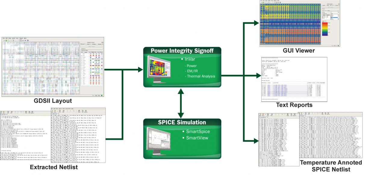
If you have a transistor-level design then we use SmartSPICE as the simulation engine to produce the power analysis numbers. Typically getting pure SPICE level accuracy for power integrity analysis is a challenging task. The number of measurements and capacity requirements can quickly overwhelm the interface. Tight API level integration enabled us to deliver the capacity and speed needed to make block level EM/IR using a designers existing SPICE netlist and GDSII a reality.

Q: What kind of results come out of your analysis tools?
For EM analysis we report any violations, and then it’s up to you for fixing the violations by using a layout editor, we do highlight the interconnect segments for quick identification. Then you would rerun analysis after making your layout fixes.
Our tool provides several reports and it even has an API so that you can see a very low-level annotation of the results at Cells, pins, ports, nets or net segments.
Q: How long does analysis take to run?
In layout mode InVar is capable of completing IR drop analysis for an average design block within several minutes. InVar runs on a single host using multiple threads, producing almost linear results depending on the number of CPUs. We’ve even used up to 64 cores on designs with millions of instances.

Q: What is the learning curve like for InVar?
It’s a simple tool to learn and run, using standard format input files. We include demo scripts in Tcl with something like 50 lines of code to help automate the process for you, and there’s a demo design for learning. You can learn how to do IR drop analysis quite quickly.
Q: When should I be concerned about power, EM/IR and thermal issues for my IC design?
Probably starting at the 28 nm node and lower process geometries for digital designs, and of course for FinFET designs because current density effects reliability, the DFM rules are very complex. Even at the 180 nm node is you are doing high current designs in LDMOS then EM rules and thermal issues need to be analyzed.
Q: Why should I consider using InVar in my IC design flow?
Our tool is very easy to use, has proven accuracy of results, provides fast analysis run times, and has an affordable price. You can check out an introduction video:
We are also going to be at TSMC OIP on September 17, and I will be available at the show all day in Booth 414. I will also present an InVar webinar before the end of September and those interested will be able to register from the Silvaco web site.
Related – Analysis of Power, Thermal, EM, IR at DAC
Related – Silvaco Swallows Invarian
Share this post via:

![SILVACO 051525 Webinar 400x400 v2[62]](https://semiwiki.com/wp-content/uploads/2025/04/SILVACO_051525_Webinar_400x400_v262.jpg)


Comments
There are no comments yet.
You must register or log in to view/post comments.