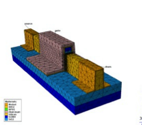
 At the most basic level, semiconductor design is all about transistors. Any report on a large microprocessor or mobile application processor is in awe about how many transistors it contains. Moore’s Law is all about the most economic way to manufacture transistors. Each process generation for the last decade and looking ahead is built around new transistor types: strained silicon, Hi-K metal gate, FinFET, FD-SOI, silicon nanotubes, carbon nanotubes, spintronics. Outside of SoC memory architectures have always been about transistors, deep trench DRAM, vertical Flash. Power (high voltage) is moving to new materials such as SiC and GaN.
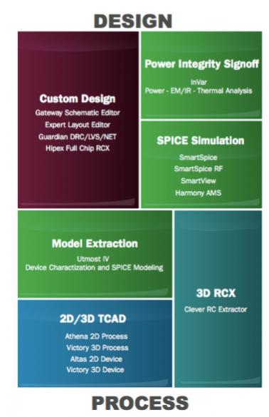
The transistor starts with the process. Technology CAD (TCAD) is the method of building up the transistor according to the process recipe and then analyzing the resulting transistor(s) to gradually converge on the desired characteristics.

The TCAD models are too slow and unwieldy to be used directly for design, a model extraction phase is required whereby the results of many TCAD characterization runs are coalesced to create a SPICE model that can be used in simulation and PDKs to allow larger designs to be undertaken.
The next level up is a traditional analog (or custom digital) flow. This consists of a high capacity layout editor (some cells are small, but others such as memories or flat-panel-displays are huge), a full 3D field-based extractor to get all the precise parasitics, and then accurate SPICE circuit simulation that can take the models from TCAD (or silicon characterization) and produce the usual performance data.
One level up from there is the requirement for full power integrity analysis: current droop due to resistance (IR drop), electromagnetic effects (EM) and thermal effects (heating due to design activity). For the most extreme environments, such as space or even avionics, single-event effects and threshold drift due to dose over time may also be required.

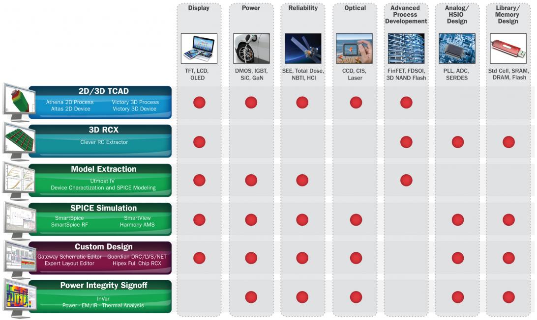
These transistor technologies can be applied to provide solutions in a wide variety of vertical markets. The key markets where Silvaco’s suite of products is used are:
- Displays: this includes TFT, LCD and OLED
- Almost all manufacturers of displays use the Silvaco suite for design and most of these designs are in high-volume manufacturing.
- Power (high voltage/current): including DMOS, IGBT, SiC and GaN
- Recently silicon-carbide (SiC) and gallium-nitride (GaN) and other materials have started to gain attention. Their wide bandgap means that they should have better performance than silicon. But that wide bandgap also leads to some challenges in simulation since accuracy needs to be very high.
- Radiation and soft error reliability: SEE, SEGR, total dose
- High energy particles cause two big problems. First, single-event-effects (SEE) including single-event-burnout (SEB) and single-event-gate-rupture (SEGR). A second effect is that the build up of the dose of radioactive particles can cause threshold shifts in the transistors which can result in long-term reliability issues.
- Optical: including CCD, CIS, solar, silicon photonics and laser
- The optical segment deals with the design of semiconductor devices that interact optically with the environment, either where light is an input (such as optical sensors) or where light is an output (such as semiconductor lasers).
- Advanced CMOS process development: FinFET, FD-SOI and more advanced
- Design of advanced CMOS processes starts with TCAD. It is too slow and expensive to run real wafers until relatively late, and much better to use rapid prototyping in TCAD to decide on an integrated flow followed by detailed simulation to determine process recipe details.
- Analog and high-speed I/O design: PLL, ADC, SERDES etc
- The real world is analog and as more and more of a system is integrated onto a single SoC, the requirement for high accuracy analog design in a mainstream processes becomes increasingly acute. At the same time, digital interfaces such as SERDES have to be designed as analog blocks.
- Foundation library and memory design: standard cell, SRAM, DRAM, flash
- One of the critical aspects of bringing a new process into production is getting the foundation IP designed (at a minimum, standard cells and SRAM memories).
Today Silvaco brought their new website online. This reflects the emphasis on these 6 vertical markets. The navigation is now across the top. A good place to start is to click on “Solutions Overview” and you will see the graphic above. This is clickable for both the technologies involved (down the left hand side) and for the vertical markets (across the top).

Silvaco will be back at DAC for the first time in a decade or more. They will be on booth 532. If you are coming to DAC then come by and see how Silvaco’s TCAD to Signoff technologies can help you in your own vertical markets.
Silvaco’s new website is here.
Share this post via:

![SILVACO 051525 Webinar 400x400 v2[62]](https://semiwiki.com/wp-content/uploads/2025/04/SILVACO_051525_Webinar_400x400_v262.jpg)


Comments
There are no comments yet.
You must register or log in to view/post comments.