![SILVACO 051525 Webinar 400x400 v2[62]](https://semiwiki.com/wp-content/uploads/2025/04/SILVACO_051525_Webinar_400x400_v262.jpg)

In order to beat Moore’s Law NAND Flash memories have moved from a planar topology to 3D construction. This allows for increased memory sized in much the same way a multistory building provides more building square footage on the same size building lot. Just like in building construction, adding a third dimension to the mix increases complexity in almost every way. Some 3D NAND designs go up to 64 devices high. Observing the problems encountered is a bit like watching a 3D chess game. The only way to understand all the read and write behaviors along with issues like program disturb errors that cause a shift in the threshold voltage of adjacent memory cells, is to use advanced modeling methods to simulate what is happening at the device level.
Silvaco recently presented a webinar on the topic of optimizing the select gate transistor in 3D NAND memory cells. The presenter, Dr. Jin Cho, did an excellent job of providing an overview of the construction and operation of 3D NAND Flash memories. He started by describing the topology of 3D NAND ICs, and then he covered some of their fabrication related issues. Among these are bowing that may occur during the high aspect ratio etch of the channel. The staircase region at the end also presents challenges during its construction. Finally, there is film deformation that can occur after the slit etch.
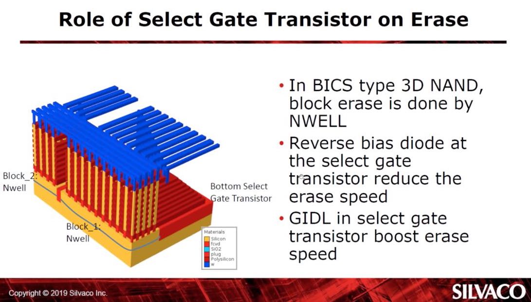
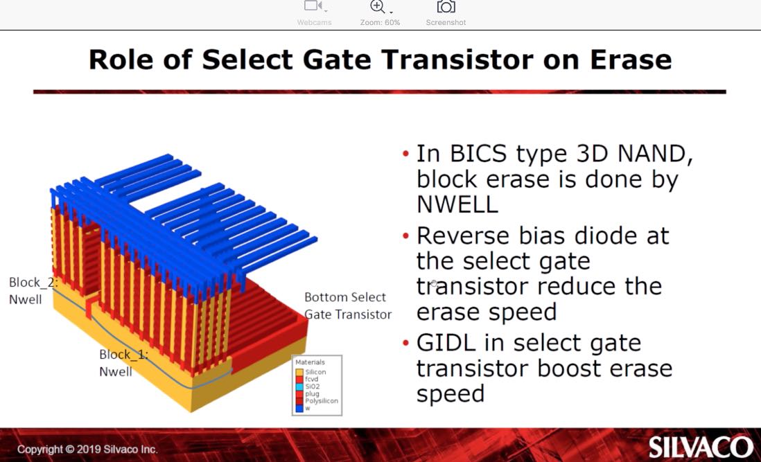
Dr. Cho talked about the large top and bottom select gate transistors, and the dummy gates that are required to prevent coupling to the active gates. Together they consume a lot of the column height, limiting space for the active gates. However, the best way to precisely know the optimal topology is to perform detailed TCAD modeling and simulation. For the purposes of the webinar Dr. Cho constructed a full 3D structure for simulation. It included implantation and diffusion. He omitted oxidation and nitridation. To properly model disturb phenomena he included at least 4 cell strings. For the TCAD device simulation he used the FN tunneling model for the write/erase operations, band to band tunneling model for the gate-induced-drain-leakage (GIDL) characteristics, and trap assistant leakage model for leakage current simulation.
Silvaco offers a cell mode simulation for the circular shape of the channel region. Without this, using voxels, a choice must be made between slow but accurate results with ~1nm resolution, or fast but inaccurate results resolution at ~5nm. Cell mode means no tradeoffs with high precision shape and fast computation times. He emphasized that this approach fits well with 3D NAND simulation needs.
The webinar then covered the details of the cell characteristics. After this the simulation for worst case read D0 and D1 conditions are discussed illustrating how the entire bit line contributes to cell behavior. The program operation was analyzed as well to set the stage for talking about program disturb. In 3D NAND there are three cases for program disturb – X, Y, XY. The net result of Dr Cho’s detailed analysis presented in the webinar is that using dummy gates strongly improves program disturb behavior. Also, it is shown that increasing the channel in the bottom select transistor reduces leakage and increases GIDL which has beneficial effects on erase speed.
The webinar, which can be easily viewed in replay, goes into much more depth than can be provided here, and is easily worth viewing if you are interested in the details of 3D NAND performance optimization. I suggest going to the Silvaco website to view the replay in its entirety.
Share this post via:


Comments
There are no comments yet.
You must register or log in to view/post comments.