

Taiwan Semiconductor Manufacturing Company Limited (TSMC) is the world’s leading dedicated semiconductor foundry, with a broad portfolio spanning from legacy nodes to the most advanced nanosheet transistor technologies. TSMC has maintained a consistent in-house R&D strategy since its founding in 1987, enabling the company to pioneer multiple industry firsts in process technology.
Historical Context
The evolution of TSMC’s logic technologies reflects the semiconductor industry’s adherence to Moore’s Law—the observation that transistor density doubles approximately every two years, improving performance and efficiency while reducing costs. As the company notes:
“Moore’s Law has not only been an observation but also a self-fulfilling prophecy guiding the semiconductor industry.”
From its early work on 3.0µm and 1.5µm processes to becoming the first foundry to mass-produce 7nm and 5nm nodes, TSMC has consistently driven the leading edge of semiconductor manufacturing.
Advanced Nodes
A14 Technology
Designed for AI-driven workloads and next-generation smartphones, A14 offers up to a 15% speed boost or 30% power reduction versus N2, with a >20% density improvement.
“A14 development is progressing smoothly with yield performance ahead of schedule.”
A16 Technology
Incorporates nanosheet transistors with Super Power Rail and a backside contact scheme, improving density and IR drop performance. Best suited for HPC products.
2nm (N2)
TSMC’s first nanosheet transistor node, offering leading performance and efficiency.
“Major customers already completed 2nm IP designs and started silicon validation.”
Recent High-Volume Production
-
3nm (N3) – Industry’s most advanced FinFET process; includes N3E, N3P, N3X, N3C, and N3A variants.
-
5nm (N5) – Second EUV node; includes N5P, N4P, N4C, N4X, and N5A for HPC and automotive.
-
7nm (N7) – First foundry EUV process (N7+), with N6 and N6e derivatives.
Mainstream & Mature Nodes
-
16/12nm FinFET – Introduced in 2013; still competitive for mobile, IoT, and automotive.
-
28nm – A versatile, cost-effective platform for smartphones, IoT, and automotive radar.
-
0.18µm – Long lifecycle applications in automotive, industrial, and mixed-signal.
Strategic Approach
TSMC emphasizes a dual focus: pushing cutting-edge AI/HPC nodes while sustaining mature, high-volume processes. This broad market coverage allows the company to serve both premium computing applications and cost-sensitive markets.
“Because of its ‘building in-house R&D’ strategy and continuous investment in R&D, TSMC is a semiconductor technology leader, helping companies around the globe unleash their IC innovations.”
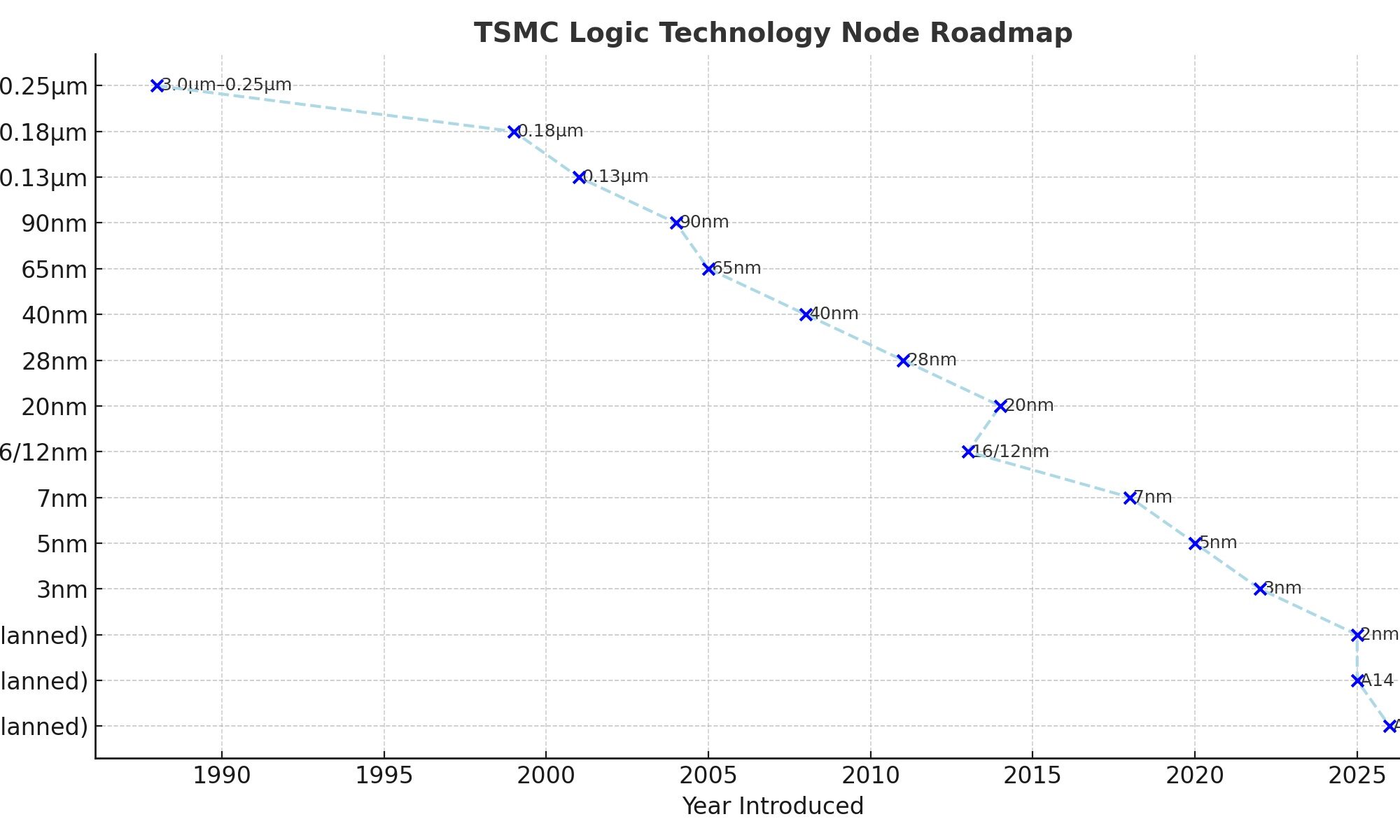
Chronological Technology Node Milestones
| Year | Node | Key Features & Breakthroughs | Main Applications |
|---|---|---|---|
| 1988–1999 | 3.0µm → 0.25µm | Transition from transferred tech to fully in-house R&D; world’s first 0.18µm low-power process (1999). | General ICs, consumer electronics |
| 2001–2004 | 0.13µm → 90nm | First low-k copper SoC; immersion lithography at 90nm. | Mobile computing, consumer devices |
| 2005–2008 | 65nm → 40nm | Low-power and mixed-signal capabilities; smallest SRAM (0.242µm²) record at 40nm. | CPUs, GPUs, game consoles, IoT |
| 2011 | 28nm | Broad portfolio (HPC, ULP, automotive, RF); leading IoT platform. | Smartphones, IoT, automotive radar |
| 2013–2016 | 16nm / 12nm FinFET | First foundry FinFET; cost-optimized 16FFC, later 12FFC+. | Mobile, AI edge, automotive |
| 2014 | 20nm | First double-patterning production, fastest ramping node. | Mobile APs, networking |
| 2018–2020 | 7nm (N7, N7+) & 5nm (N5) | First EUV foundry node (N7+); second EUV node (N5) with HPC and automotive variants. | HPC, smartphones, automotive |
| 2022 | 3nm (N3) | Most advanced FinFET with N3E, N3P, HPC-focused N3X. | HPC, premium smartphones |
| 2025 (planned) | 2nm (N2) | First nanosheet transistor node, major efficiency and density gains. | Energy-efficient computing, HPC |
| 2026+ (planned) | A14 / A16 | Nanosheet + NanoFlex Pro; SPR backside power delivery; tuned for AI/HPC. | AI accelerators, HPC, advanced mobile |
Strategic Approach
-
Dual Focus – Maintain leadership in bleeding-edge AI/HPC nodes while supporting mature nodes for high-volume, cost-sensitive markets.
-
Variant Expansion – Extend each node with enhanced, power-optimized, cost-effective, and application-specific derivatives.
-
Global Infrastructure – Aligns new node rollouts with long-term fab capacity planning in Taiwan and overseas.


CEO Interview with Jerome Paye of TAU Systems