

TSMC 3D Fabric™ is a comprehensive suite of 3D silicon stacking and advanced packaging technologies developed by Taiwan Semiconductor Manufacturing Company (TSMC) to enable high-performance, power-efficient, and space-optimized system integration. It represents TSMC’s response to growing industry demand for heterogeneous integration, chiplet-based designs, and next-generation computing workloads in AI, HPC, mobile, and networking.
Introduced under a unified brand, TSMC 3D Fabric integrates front-end and back-end 3D technologies—SoIC™ (System on Integrated Chips), InFO™ (Integrated Fan-Out), and CoWoS® (Chip-on-Wafer-on-Substrate)—to provide design flexibility and performance scaling beyond traditional monolithic SoC scaling limits.
Overview
As Moore’s Law slows and system complexity grows, advanced packaging has become essential for future innovation. TSMC 3D Fabric™ allows designers to:
-
Integrate chiplets with different process nodes (e.g., N3, N5, N7)
-
Combine logic, memory, analog, and I/O dies into a single package
-
Achieve higher bandwidth, lower latency, and better energy efficiency
-
Enable fine-pitch interconnects and shorter signal paths
-
Optimize for cost, yield, and design modularity
TSMC 3D Fabric supports both 2.5D and 3D IC architectures, making it adaptable for high-performance computing (HPC), AI accelerators, 5G infrastructure, AR/VR, and automotive applications.
Core Technologies
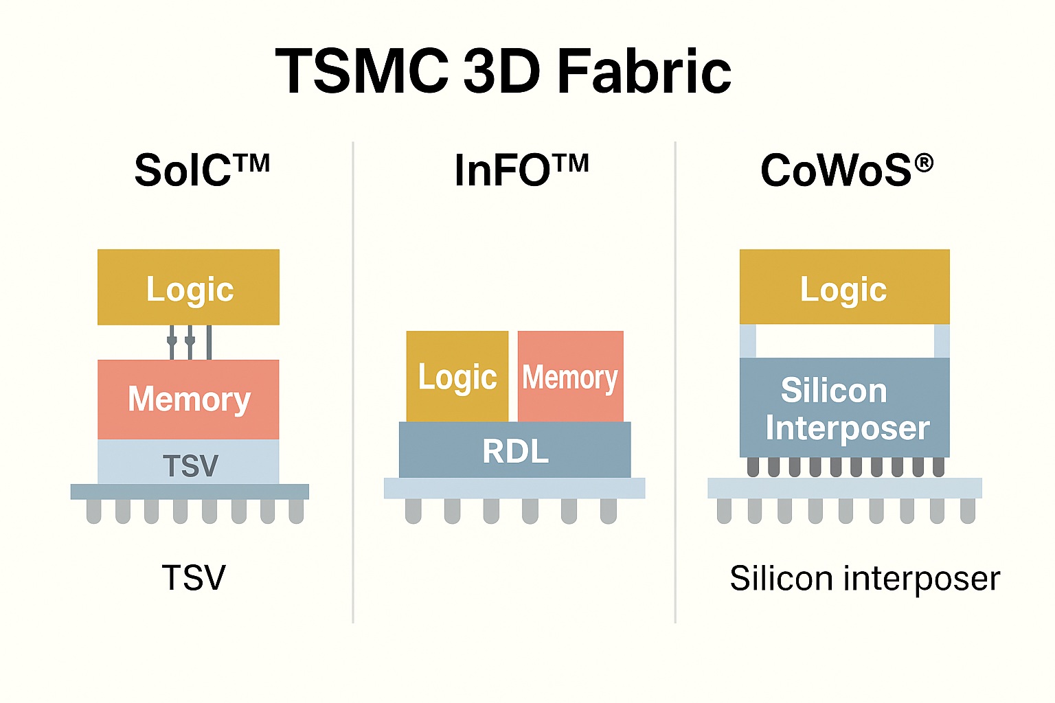
1. SoIC™ (System on Integrated Chips) – 3D IC
SoIC is TSMC’s front-end 3D chip stacking technology.
-
Die-to-die bonding with high-density through-die vias (TSVs) and direct copper-to-copper hybrid bonding
-
Vertical stacking of logic or memory dies (face-to-face or back-to-face)
-
Enables integration across process nodes (e.g., stacking N7 + N3)
-
Offers sub-10μm bump pitches and high interconnect density
-
Used in TSMC-SoIC®+InFO/CoWoS® hybrid packages
Applications: CPU + SRAM stacking, high-bandwidth AI cores, logic-on-logic stacking, cache-on-logic for latency-critical systems
2. CoWoS® (Chip-on-Wafer-on-Substrate) – 2.5D Integration
CoWoS is a back-end advanced packaging solution for side-by-side integration on a silicon interposer.
-
Uses a large silicon interposer to connect multiple dies (logic, memory, analog)
-
High-density RDL and fine-pitch interconnects
-
Supports HBM integration, high-speed die-to-die interfaces
-
CoWoS-L, CoWoS-S, and CoWoS-R variants offer different scaling and power profiles
Applications: HPC GPUs, AI accelerators (e.g., Nvidia, AMD), networking ASICs
3. InFO™ (Integrated Fan-Out) – 3D/2.5D for Mobile & Low-Power
InFO provides a compact, cost-effective alternative to interposers.
-
Uses a reconstituted wafer with fan-out redistribution layers (RDLs)
-
Allows die stacking (InFO-POP), side-by-side die placement (InFO_SoW), and memory-on-logic
-
Ultra-thin form factor for smartphones and edge AI
Variants include:
-
InFO_PoP: Logic and DRAM stacking for mobile APs
-
InFO_oS: Optimized for SoC and RF integration
-
InFO_L: Large-die fan-out for edge devices
Applications: Mobile SoCs (Apple A-series), edge AI, AR/VR chips
TSMC 3D Fabric Architecture
TSMC promotes a “More than Moore” and “System Integration” philosophy, enabling:
-
Heterogeneous integration across different process technologies (FinFET, N3, N5, RF, analog)
-
Customizable chiplet partitioning strategies
-
Power and thermal optimization using stacked or adjacent die placement
-
Modular design reuse for faster time-to-market
Manufacturing and Ecosystem
-
SoIC and CoWoS are fabricated in TSMC’s advanced backend facilities (e.g., Fab 6, Fab 20)
-
InFO is manufactured on reconstituted wafers using wafer-level packaging
-
Ecosystem partners include EDA vendors (Synopsys, Cadence, Siemens), IP providers, and design houses
-
TSMC also supports Open Innovation Platform® (OIP) for 3D Fabric design enablement, toolkits, and IP qualification
Notable Use Cases & Customers
-
Apple: InFO for A-series mobile processors
-
AMD: CoWoS for high-performance GPUs and accelerators
-
Nvidia: CoWoS with HBM for AI training chips (e.g., A100, H100)
-
TSMC + SoIC: Next-gen HPC and logic stacking (e.g., Arm Neoverse chiplets)
-
TSMC partners with Broadcom, Intel, and Google on advanced packaging pilots
Advantages
| Feature | Benefit |
|---|---|
| 3D stacking | Maximized bandwidth, minimized latency |
| Chiplet integration | Flexible reuse, improved yield |
| Fine-pitch interconnects | High density at lower power |
| Design modularity | Easier upgrade cycles |
| Cross-node support | Combine mature and cutting-edge nodes |
Challenges
-
Thermal management for stacked logic dies
-
Testability and yield analysis of multi-die systems
-
Design complexity in 3D integration flows
-
Supply chain readiness for mass production
-
Cost sensitivity for mainstream markets
Future Directions
-
Expansion of TSMC-SoIC-Direct for ultra-high-performance 3D ICs
-
Wafer-on-wafer (WoW) and chip-on-wafer-on-wafer (CoWoW) research
-
Hybrid bonding at <6μm pitch
-
Integration of photonics, memory, and power delivery within 3D Fabric
-
Co-optimization with backside power delivery and High-NA EUV nodes
Also Read:


Captain America: Can Elon Musk Save America’s Chip Manufacturing Industry?