

Gigafab is a term used in the semiconductor industry to describe an ultra-large semiconductor fabrication plant (fab) capable of producing wafers at a scale exceeding 100,000 wafer starts per month (WSPM). These facilities represent the pinnacle of scale, automation, and capital intensity in advanced chip manufacturing. The term is most commonly associated with Taiwan Semiconductor Manufacturing Company (TSMC), which pioneered the concept and terminology to reflect its world-leading manufacturing capacity.
Overview
-
Definition: A Gigafab is a semiconductor fabrication plant with a monthly production capacity exceeding 100,000 300mm wafers. It typically features the most advanced process technologies and extreme automation systems.
-
Purpose: Gigafabs enable economies of scale in the production of advanced semiconductors, especially for high-volume markets like mobile, AI, HPC, and automotive.
History
-
Coined by TSMC: The term “Gigafab” was introduced by TSMC in the late 2000s to differentiate its largest fabs from traditional manufacturing plants. TSMC’s goal was to align with its aggressive capacity expansion strategies and leadership in foundry manufacturing.
-
First Gigafab: TSMC’s Fab 12 in Hsinchu, Taiwan, was one of the earliest fabs to reach “gigafab” capacity.
-
Subsequent Gigafabs: The concept expanded to include Fab 14 and Fab 15 in Tainan, Fab 18 (advanced 5nm/3nm production), and more recently Fab 20, part of TSMC’s Arizona expansion.
Key Characteristics
| Feature | Description |
|---|---|
| Wafer Size | 300mm (12-inch) |
| Monthly Output | >100,000 wafers |
| Process Nodes | Advanced nodes (5nm, 3nm, 2nm, and beyond) |
| Automation | Extreme automation with AI-based predictive systems, AGVs, and advanced MES |
| Cleanroom Area | Often over 100,000 square meters |
| Investment Scale | Typically $10–20+ billion per facility |
| Production Type | Mostly logic (CPUs, GPUs, SoCs) and recently high-density 3D ICs |
Notable Gigafabs
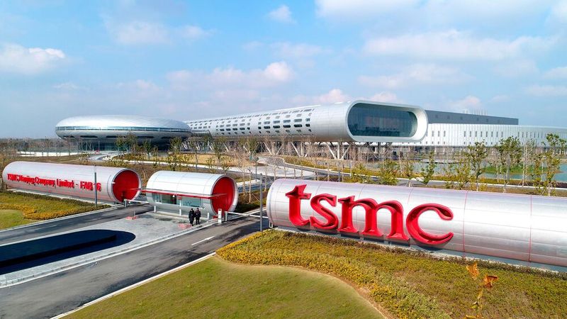
🇹🇼 TSMC – Taiwan
-
Fab 12 (Hsinchu Science Park): One of the first gigafabs; major 65nm to 16nm production.
-
Fab 14 (Tainan Science Park): Expanded capacity for 40nm to 16nm chips.
-
Fab 15 (Tainan): Initially 28nm; upgraded to 16nm and 7nm.
-
Fab 18 (Tainan): Core 5nm and 3nm hub; future N2 (2nm) production.
-
Fab 20 (Arizona, USA): Part of TSMC’s overseas gigafab strategy; focused on 4nm and 3nm.
🇺🇸 Intel – USA
While Intel does not use the term “Gigafab,” some of its campuses like Ocotillo (Arizona) and the new Ohio mega-site are functionally gigafabs due to their size and capacity plans.
🇰🇷 Samsung – Korea
Samsung has multiple large-scale fabs in Hwaseong and Pyeongtaek that meet or exceed Gigafab scale, including fabs focused on leading-edge EUV-based 3nm and 2nm production.
Technological Importance
Gigafabs are vital to:
-
Advanced Packaging Integration: Supporting 2.5D/3D stacking and chiplet-based SoCs.
-
EUV Lithography Deployment: Housing EUV tools for sub-5nm processes.
-
Foundry Ecosystems: Acting as cornerstones for ecosystems like TSMC’s Open Innovation Platform (OIP).
-
Capacity Buffering: Serving global tech giants with reliable high-volume output (e.g., Apple, Nvidia, AMD, Qualcomm).
Challenges
-
Capital Expenditure: Requires $10B–$25B+ per facility.
-
Skilled Labor: Needs a large, highly-trained workforce.
-
Supply Chain Resilience: Dependent on rare materials and precise equipment logistics.
-
Geopolitical Risks: Concentration in specific regions (like Taiwan) raises concerns about supply security.
Future Trends
-
Global Expansion: New Gigafabs planned in Japan, USA (Arizona, Ohio), and Europe.
-
3D IC Integration: Gigafabs increasingly support advanced packaging (CoWoS, Foveros, SoIC).
-
Sustainability Focus: Investments in green fabs using recycled water and renewable energy.Also Read:


CEO Interview with Jerome Paye of TAU Systems