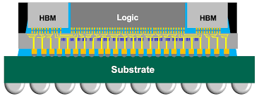
CoWoS® (Chip-on-Wafer-on-Substrate) is a 2.5D advanced packaging technology developed by TSMC that allows multiple dies—including logic, memory, and analog ICs—to be integrated side-by-side on a high-density silicon interposer. CoWoS is a cornerstone of TSMC’s 3D Fabric™ platform and plays a critical role in enabling high-performance computing (HPC), AI accelerators, networking ICs, and advanced SoCs.
Introduced in the early 2010s and continually enhanced since, CoWoS enables significantly higher bandwidth, lower latency, and more efficient power delivery compared to traditional package-level integration methods. It is widely adopted by leading semiconductor companies such as Nvidia, AMD, Broadcom, and Apple.
Overview
Traditional printed circuit boards (PCBs) or organic substrates have limited wiring density, signal integrity, and thermal performance. As Moore’s Law slows and monolithic SoCs reach reticle size and yield limits, 2.5D integration via CoWoS allows chip designers to partition large dies into smaller chiplets and reassemble them in a unified package, improving yield and modularity while achieving near-monolithic performance.
CoWoS uses a passive silicon interposer—etched with thousands of fine interconnects—that sits between the active dies and the package substrate. This interposer provides high-density connections between chiplets and supports memory integration, most notably High Bandwidth Memory (HBM) stacks.
Key Features
| Feature | Description |
|---|---|
| 2.5D Integration | Side-by-side dies placed on a silicon interposer (not stacked) |
| High Interconnect Density | ~micron-scale pitch interconnects via RDL and TSVs |
| High Bandwidth | Supports HBM2, HBM2e, HBM3 with wide bus interfaces |
| Thermal Efficiency | Efficient heat dissipation with thermal vias and copper blocks |
| Modular Design | Enables heterogeneous chiplets across nodes and fabs |
| Co-Design Friendly | Compatible with logic, analog, RF, memory integration |
| Production-Proven | Mass production since ~2013 for Nvidia, Xilinx, etc. |
Architecture and Flow
CoWoS involves a multi-step fabrication process:
-
Chiplets (Dies) are fabricated separately—can be logic, memory, analog, or custom accelerators.
-
Silicon interposer is fabricated with through-silicon vias (TSVs) and redistribution layers (RDLs) to route signals.
-
Dies are placed side-by-side and bonded onto the interposer using micro-bumps or hybrid bonding.
-
The entire wafer assembly is then attached to a package substrate, which connects to the PCB.
-
Encapsulation, testing, and thermal solutions are added.
CoWoS Variants
TSMC has developed several versions to support diverse applications:
CoWoS-S (Standard)
-
Traditional 2.5D integration with interposer between logic and HBM
-
Widely used in HPC and networking chips
CoWoS-L (Large Interposer)
-
Supports reticle-size interposers and ultra-large packages
-
Used in AI training accelerators requiring multiple HBMs and large logic dies
CoWoS-R (Redistributed Interposer)
-
Uses RDL technology to reduce interposer cost
-
Suitable for smaller dies or high-volume applications
CoWoS-X / CoWoS-2.0 (Advanced)
-
Hybrid bonding, improved power delivery, tighter pitches
-
Next-gen design under research to enable even higher interconnect density
Applications
-
AI Accelerators: Nvidia H100, B100 (HBM3 via CoWoS)
-
Networking ASICs: Broadcom Tomahawk, Jericho
-
HPC GPUs and CPUs: AMD Instinct MI series
-
Custom ASICs: Google TPU, Amazon Trainium/Inferentia
-
Advanced SoCs: Combining analog, RF, logic, and memory on one platform
CoWoS vs Other Technologies
| Feature | CoWoS | InFO | SoIC | Intel EMIB | Samsung I-Cube |
|---|---|---|---|---|---|
| Type | 2.5D | Fan-out | 3D | 2.5D bridge | 2.5D |
| Interposer | Silicon | None | None | Embedded bridge | Silicon |
| Bandwidth | Very High | Medium | Ultra High | High | High |
| Cost | Higher | Lower | Highest | Medium | Medium |
| Memory Support | Yes (HBM) | No | Yes | Yes | Yes |
Advantages
-
Near-monolithic performance with modular benefits
-
Enables chiplet disaggregation and reuse
-
Excellent signal integrity and power delivery
-
Proven path to integrate HBM memory
-
Scalable for massive dies across multiple reticles
Challenges
-
Expensive interposer manufacturing
-
Thermal management of dense logic+HBM configurations
-
Package yield and assembly complexity
-
Requires deep co-design with substrate, interposer, and silicon teams
Future Directions
-
Integration with SoIC (3D stacking) for vertical logic-memory stacking
-
Adoption of hybrid bonding for sub-10μm pitch interconnects
-
Larger CoWoS packages for AI clusters and supercomputing
-
Co-design with TSMC N2 / N3 nodes and HBM4
-
Enabling open chiplet ecosystems via UCIe compatibility
Also Read:
Share this post via:


Captain America: Can Elon Musk Save America’s Chip Manufacturing Industry?