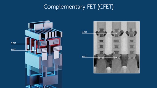
A Complementary FET (CFET) vertically stacks the n-FET and p-FET of a CMOS pair on top of each other (often as stacked nanosheets), collapsing the lateral n–p spacing in today’s standard cells. By “folding” CMOS into the vertical dimension, CFET targets major area and routing wins at future logic nodes while preserving strong electrostatics from gate-all-around (GAA) devices.
Imec formally placed CFET on the logic roadmap for the beyond-1 nm era and has pursued both monolithic and sequential integration schemes to realize it.
Device architecture at a glance
-
Stacked channels: n- and p-type nanosheets (or nanowires) are vertically stacked and independently gated. This eliminates lateral n–p separation as the primary cell-area limiter.
-
Monolithic CFET: Both polarities built on one wafer with careful process sequencing, epi, isolation and contacts. Imec has shown electrically functional monolithic CFETs with stacked bottom and top source/drain contacts.
-
Sequential CFET: Build one polarity, bond/transfer a second wafer, then build the other polarity under a low-temperature budget. Progress in wafer-to-wafer hybrid bonding (pitches headed toward ~250 nm) is a key enabler.
Bridging path: Nanosheet → Forksheet → CFET
The industry is extending GAA nanosheets and inserting forksheet devices as a bridge to CFET. In 2025, imec moved from an “inner-wall” to an outer-wall forksheet for better manufacturability while preserving area/performance gains, explicitly positioning forksheet to bridge nanosheet and CFET around the A10 node.
DTCO and standard-cell evolution
CFET’s biggest wins land at the standard-cell level:
-
Track-height shrink: Imec’s CFET work targets moving from 5T to 4T and below (and with a new double-row CFET cell, even 3.5T) without performance loss, by combining CFET with backside power/signal techniques.
-
Double-row CFET cell (IEDM 2024): A DTCO study found a two-row CFET with a shared middle routing wall simplifies MOL connectivity and cuts logic/SRAM area; imec also demonstrated a functional monolithic CFET with direct backside contact to the bottom device as a key building block.
Materials and channel options
Baseline CFET studies use Si/SiGe nanosheets, but multiple groups—and imec explicitly—are exploring 2D (atomically thin) channels (e.g., WS₂/MoS₂) inside advanced CFETs to push scaling further into the Å-era. A 2025 review outlines a roadmap to 2D-material CFETs and the associated integration challenges.
Key process & design challenges
-
Overlay/alignment: Sub-3 nm top–bottom overlay accuracy is needed for stacked contacts/gates (recent imec experiments report tight overlay for backside-patterned contacts).
-
Thermal budgets: Especially for sequential CFET, low-temperature processing is required to avoid degrading the pre-built device during the second build. (Hybrid bonding and low-T MOL stacks are active areas.)
-
Contacts and MOL: Achieving stacked S/D and self-aligned contacts with acceptable resistance and parasitics is central; first demonstrations of stacked unipolar top/bottom FETs and monolithic CFETs have de-risked this.
-
Backside power & buried power rails (BPR): CFET’s routing density pairs naturally with backside power delivery, which relocates power rails and frees frontside tracks for signals. (DTCO studies since 2019 have highlighted BPR/BSPD as scaling boosters beyond N3.)
State of the art (selected milestones)
-
2018 (VLSI): Imec presents a CFET process flow “for nodes beyond N3,” projecting ~50% potential area reduction for standard cells/SRAMs vs. FinFET approaches.
-
2023–2024 (IEDM/VLSI): Demonstrations of stacked top/bottom devices and monolithic CFETs with stacked or backside contacts; imec shows electrically functional CFET devices. 2024 (IEDM): Imec proposes a double-row CFET standard cell, reducing cell height from 4T to 3.5T and simplifying MOL. imec
-
2025 (VLSI): Outer-wall forksheet unveiled as the manufacturable bridge to CFET at A10, extending nanosheet era while CFET matures.
Timeline & outlook
Multiple imec sources and industry coverage align on A7 (~0.7 nm-class) around ~2031 as the earliest mass-production window for CFET, with A10 (≈1 nm) still the realm of nanosheet/forksheet. Expect forksheet-based cells first, then CFET as backside power, MOL, and bonding overlays harden. (Roadmaps vary by company; the dates are research-driven estimates, not foundry commitments.)
Notable quotes
-
“CFET is an attractive device architecture for beyond 1 nm logic technology nodes.”
-
“This makes CFET mass production feasible only from the A7 node onwards, according to imec’s roadmap.” — imec on forksheet → CFET timing.
-
“In CFETs, the idea is to stack both nFET and pFET wires on each other… eliminating the n-to-p separation bottleneck.”
-
“Our DTCO study shows that one shared [routing] wall for every 3.7 FET is sufficient… [cutting] standard cell heights from 4 to 3.5T.”
-
“The forksheet… bridges nanosheet and CFET device architectures.”
See also
GAA nanosheets, Forksheet devices, Backside Power Delivery (BSPD) & Buried Power Rails (BPR), Hybrid bonding, 2D-material channels.


Chemical Origins of Environmental Modifications to MOR Lithographic Chemistry