

Chip-on-Panel-on-Substrate (CoPoS) is an advanced packaging architecture that “panelizes” the classic chip-on-carrier flow. Instead of building redistribution and interposer structures on round wafers, CoPoS forms them on large rectangular panels, then mounts the finished module onto an organic or glass package substrate. The goal is to unlock larger package sizes, higher integration density, and better cost per square millimeter than wafer-only approaches, especially for AI/HPC systems that need multiple compute chiplets and many stacks of high-bandwidth memory (HBM).
Key idea: bring the area and throughput economics of panel-level processing to packages that previously depended on wafer-scale silicon interposers.
Why it matters
-
Scale beyond reticle limits: Very large systems-in-package exceed single-reticle dimensions; panel carriers provide the physical real estate to stitch massive interconnect planes.
-
Cost efficiency at size: Square panels reduce edge scrap and improve utilization versus circular wafers, helping the economics of extra-large packages.
-
Flexibility of materials: CoPoS enables organic or glass-core “panel interposers” (or thick RDL cores) as alternatives/adjuncts to silicon interposers, balancing density, loss, flatness, and cost.
-
AI/HPC ready: As model sizes and memory footprints grow, CoPoS supports more chiplets, more HBM stacks, and higher I/O counts without a radical redesign of the end substrate.
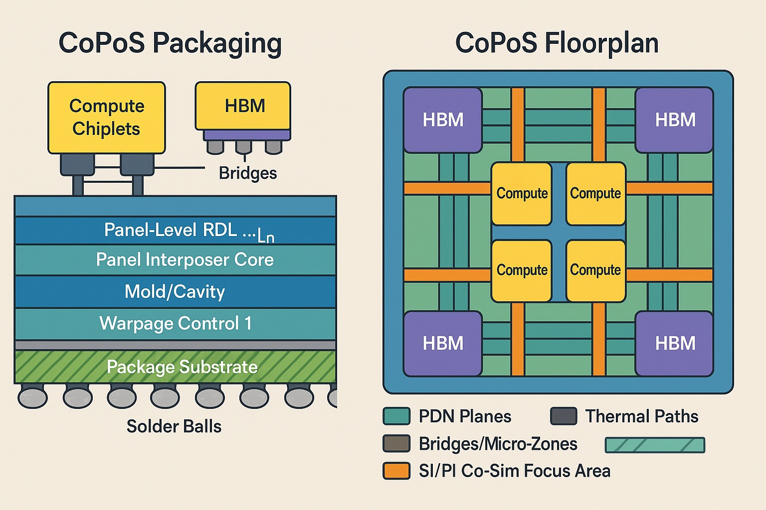
Typical stack & flows
A generic CoPoS stack looks like this (top to bottom):
-
Compute chiplets / accelerators / controllers
-
HBM or other stacked memories
-
Panel interposer / panel RDL (organic or glass core with fine redistribution, or a fan-out style RDL build-up on panel)
-
Cavity mold / underfill / warpage-control layers as required
-
Package substrate (high-density organic or glass), then solder balls / lands to the board
Process variants you’ll hear about:
-
Chip-first panel fan-out: Place die on a panel carrier, encapsulate, then pattern fine RDL above.
-
Chip-last panel fan-out: Build RDL first on the panel, then place/attach die to the finished interconnect.
-
Bridge-assisted panelization: Integrate silicon/organic bridges locally to push very fine pitches only where needed.
-
Glass-core panel interposer: Use glass for flatness and dimensional stability; metallize and build RDL at panel scale.
Design & technology considerations
-
Interconnect density: Organic/glass panel interposers lag silicon in ultimate line/space, but are catching up with advanced lithography and build-up dielectrics. Use bridges or localized silicon where ultra-fine pitch is mandatory.
-
Signal integrity (SI): Long panel-scale routes demand careful control of impedance, insertion loss, and skew; glass cores help with flatness and dielectric stability, while organics can be tuned with resin systems and build-up geometry.
-
Power delivery (PDN): Wide, low-inductance planes across large areas are essential. Decap placement, via farms, and return path continuity dominate early floorplanning.
-
Thermals: With many hot chiplets and tall memory stacks, you’ll need heat spreaders, vapor chambers, TIM optimization, and smart keep-out zones. Panel thickness and material CTE play into thermal-mechanical reliability.
-
Warpage & die shift: Larger panels amplify CTE mismatch. Flow selection (chip-first vs. chip-last), cure temperatures, and symmetric layer stacks are used to tame warpage.
-
Assembly & test: Known-good-die (KGD) strategy is vital. At-panel test coupons, daisy chains, and BIST hooks reduce risk before singulation.
CoPoS vs. other approaches
-
CoWoS / Si-interposer stacks: Excellent density and maturity, but silicon area and stepper time get expensive for very large packages. CoPoS seeks similar functionality with better panel economics and material flexibility.
-
Fan-Out Wafer-Level Packaging (FOWLP): Great for mobile/consumer and mid-size modules; panelizing extends the paradigm to much larger footprints.
-
EMIB/bridge-only strategies: Fine for localized ultra-dense links. CoPoS complements them by providing a large, shared RDL canvas across the whole module.
-
Glass-core substrates: CoPoS can incorporate glass as either the interposer core or the final package substrate to improve flatness and dimensional control at scale.
Integration patterns you’ll see
-
Many-to-many chiplet fabrics: Several compute dies linked by panel RDL or embedded bridges, with centrally managed clock/power grids.
-
HBM-rich floorplans: 4–12+ memory stacks distributed around compute islands; short routes from HBM to compute to keep latency and loss down.
-
Hybrid density zones: Use organic/glass for most routes, and drop in silicon bridges or RDL “micro-zones” where sub-10 μm L/S is unavoidable.
Reliability & qualification themes
-
Board-level reliability (BLR): Solder joint fatigue on very large packages is a first-order concern; corner-keepouts, dummy copper, and stiffeners help.
-
Thermo-mechanical cycling: CTE stacking (silicon ↔ mold ↔ RDL ↔ panel core ↔ substrate) requires careful symmetry and resin choice.
-
Underfill strategy: Capillary vs. non-flow underfill, fillet design, and reworkability are tuned by die size, bump pitch, and routing density.
-
Moisture sensitivity & reflow: Large panels and thick stacks call for conservative MSL control and reflow profiles to avoid delamination.
Economics & capacity levers
-
Carrier utilization: Rectangular panels reduce perimeter scrap and can fit more/larger modules per carrier than a circular wafer.
-
Throughput: Larger step area and panel handling raise raw throughput, but demand panel-scale alignment, inspection, and metrology.
-
Yield strategy: Break the design into yield-friendly chiplets; favor KGD and redundancy in the interconnect fabric; incorporate at-panel screening before final assembly.
EDA & design-enablement
-
Package-system co-design: Treat the panel interposer as an electrically significant layer stack, not just a mechanical carrier. Co-opt board tools for panel routing, and IC/package co-simulation for timing/SI/PDN.
-
Floorplan early, floorplan often: Thermals and PDN drive chiplet placement as much as signal topology. Iterate with power maps and realistic heat-sink models.
-
DFM for panel lithography: Anticipate overlay limits and local die shift; use guard-bands and stitching-tolerant topologies.
Roadmap signals (high level, no dates)
-
Migration from wafer-centric to panel-centric interposers/RDL for the very largest AI/HPC packages.
-
Increasing use of glass cores for flatness and stability, with organics continuing where cost and maturity win.
-
Wider adoption of hybrid interposers that mix panel RDL with localized silicon bridges to hit both cost and density goals.
Quick glossary
-
Panel interposer: A large organic/glass core with fine RDL that substitutes for (or augments) silicon interposers.
-
Fan-out (FO): Building RDL over mold or dielectric so signals “fan out” from the die.
-
KGD: Known-good-die, tested prior to assembly to improve module yield.
-
PDN: Power-delivery network—the planes, vias, and capacitors feeding current to the chiplets.
-
BLR: Board-level reliability—how the package survives soldering and life on the PCB.
Design checklist (practical starting points)
-
Define system limits: total I/O, bandwidth targets, allowable latency, TDP per die.
-
Choose the panel core: organic vs. glass; required line/space; flatness/CTE needs.
-
Select the flow: chip-first vs. chip-last; where to use bridges; plan for underfill and rework.
-
PDN first: allocate planes, via fields, decap islands; simulate droop and resonances early.
-
Thermals second: heat-spreader design, keepouts, TIM stack-up, and airflow model.
-
SI/PI co-sim: treat the panel as part of the channel; include vias, stubs, and return paths.
-
DFM loops: overlay budgets, die shift, panel warpage windows; add monitor structures.
-
Test strategy: at-panel coupons, KGD policies, and screening criteria before singulation.
Notable quotes
“Panel is not just a bigger canvas; it’s the economic lever that makes mega-packages practical.”
“When compute and memory scale faster than substrates, the substrate becomes the roadmap.”
“Glass buys you flatness; bridges buy you density; together they buy you yield.”
“Treat the panel like part of the chip, and the chip like part of the system.”
“The first millimeter of routing past the bump pad decides your signal integrity fate.”
“Power delivery is the real interposer—everything else rides on it.”
“CoPoS doesn’t replace silicon; it reserves silicon density for where it matters most.”
Also Read:
CoWoS® (Chip-on-Wafer-on-Substrate) Wiki
3D IC (Three-Dimensional Integrated Circuit) Wiki
Share this post via:


Things From Intel 10K That Make You Go …. Hmmmm