S2C is a leading global supplier of FPGA prototyping solutions for today’s innovative SoC and ASIC designs, now with the second largest share of the global prototyping market. S2C has been successfully delivering rapid SoC prototyping solutions since 2003. With over 500 customers, including 6 of the world’s top 15 semiconductor companies, our world-class engineering team and customer-centric sales team are experts at addressing our customer’s SoC and ASIC verification needs. S2C has offices and sales representatives in the US, Europe, mainland China, Hong Kong, Korea and Japan.
Why is prototyping important?
FPGA prototyping is the method to prototype SoC and ASIC designs on FPGAs for hardware verification and early software development.
- Running an SoC design on FPGA prototype is a reliable way to ensure that it is functionally correct. A single prototyping platform can provide verification for hardware, firmware, and application software design functionality before the first silicon pass.
- Time-to-market (TTM) is reduced from FPGA prototyping: After the design process, FPGAs are ready for production, while standard cell ASICs take more than six months to reach production.
- Early software development: Rather than waiting for the first silicon to come back, SoC design houses can leverage the FPGA prototype’s superior performance to start developing and validating their software. Such parallel software development can significantly shorten the design cycle by six to nine months.
Prodigy™ Complete Prototyping Solutions

S2C’s Prodigy Complete Prototyping Solutions addresses the need for a comprehensive solution that operates at any functional design stage, with any design size, and across multiple geographical locations. All of these capabilities are available on-demand and remotely accessible at all times. The Prodigy Prototyping Platform features:
- Shortened design to FPGA mapping time
- Leading multi-FPGA deep trace debug
- Vast library of 90+ daughter cards to meet a variety of interface needs
- The most scalable/flexible architecture for designs of various sizes, applications and stages
The Prodigy Complete Prototyping Solutions consists of the following products:
- Prodigy Logic Matrix High density FPGA Prototyping platform with hierarchical connectivity to facilitate scaling and support for hyperscale designs at prototyping performance
- Prodigy Logic Systems based on Xilinx’s Virtex UltraScale+ and Intel’s Stratix-10 and Arria-10 FPGA families
- Prodigy Logic Modules based on Xilinx’s Virtex UltraScale, Kintex UltraScale and Kintex-7 FPGA
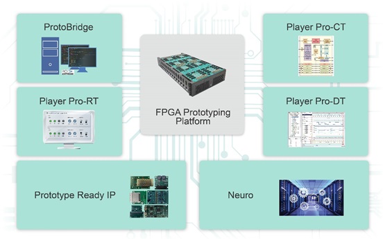
- Prodigy Player Pro™ to partition a design to multiple FPGAs, configure the prototype, and provide remote system monitoring and control
- Prodigy Multi-Debug Module The Prodigy Multi-Debug Module Pro (MDM Pro) is an innovative deep trace debugging solution for FPGA prototyping and allows concurrent debugging of multiple FPGAs.
- Prodigy ProtoBridge™ to link system-level simulation environments to FPGA-based prototyping, which enables early algorithm/architectural exploration on FPGA, accelerates design verification and increases FPGA-based prototyping test coverage
- Neuro The verification cloud solution is mainly used for the front-end functional verification of ultra-large-scale digital integrated circuits, including architecture exploration, algorithm verification, IP/module-level verification, chip-level verification, firmware verification, software verification, and compatibility testing.
- An extensive library of over 90 Prodigy Prototype Ready™ Interfaces and Accessories designed to enable users to prototype SoC designs with a variety of interfaces and work out-of-box with the S2C’s comprehensive family Logic Systems and Logic Modules
For more information, please visit www.s2inc.com or contact marketing@s2ceda.com
Share this post via:


Comments
There are no comments yet.
You must register or log in to view/post comments.