As semiconductor manufacturing becomes increasingly knowledge-intensive, protecting intellectual property and trade secrets has emerged as a strategic imperative. The world’s leading foundry, TSMC is advancing beyond conventional information security practices by integrating artificial intelligence into trade secret management. This transformation marks a significant milestone in the evolution of enterprise knowledge protection, enabling intelligent identification, classification, monitoring, and risk mitigation of critical proprietary information.
Trade secrets represent some of the most valuable assets within semiconductor organizations. Process technologies, design methodologies, equipment recipes, yield optimization techniques, materials research, and manufacturing know-how often provide competitive advantages worth billions of dollars. Traditional protection mechanisms, including access controls, document classification systems, and employee compliance programs, have become increasingly challenged by the sheer volume and complexity of digital information generated across advanced semiconductor operations.
TSMC’s AI-powered trade secret management framework addresses these challenges through the deployment of machine learning, natural language processing (NLP), and intelligent data analytics. Rather than relying solely on manual classification, AI systems continuously analyze documents, emails, technical reports, source code, process documentation, and collaborative communications to identify information that may constitute sensitive intellectual property.
A key component of this approach is semantic understanding. Modern large language models and domain-specific AI engines can recognize technical concepts, process parameters, device architectures, and manufacturing terminology associated with proprietary semiconductor technologies. This enables automated classification of sensitive content even when traditional keywords or predefined labels are absent. Such contextual awareness significantly improves the accuracy of trade secret identification while reducing administrative burden.
Another critical capability is intelligent risk detection. AI systems can monitor information flows across enterprise networks, cloud platforms, collaboration tools, and engineering databases to detect anomalous behavior. By establishing behavioral baselines, machine learning models can identify unusual access patterns, abnormal data transfers, excessive document downloads, or atypical collaboration activities that may indicate potential insider threats or unauthorized disclosure risks.
In advanced manufacturing environments, where thousands of engineers and researchers collaborate across multiple disciplines, real-time monitoring becomes essential. AI-driven analytics can evaluate risk scores dynamically, enabling security teams to prioritize investigations and respond proactively to emerging threats. This shift from reactive security management to predictive protection represents a fundamental advancement in enterprise risk management.
The integration of AI also enhances compliance and governance. Semiconductor companies operate within increasingly stringent regulatory environments that require comprehensive documentation of information security practices. AI-powered systems can automatically generate audit trails, maintain classification records, track data lineage, and provide evidence of policy enforcement. These capabilities improve transparency while supporting regulatory and legal requirements associated with trade secret protection.
From an operational perspective, intelligent trade secret management contributes to innovation acceleration. Engineers spend less time manually classifying documents and navigating security procedures, while organizations gain greater confidence in knowledge-sharing activities. AI enables a balance between collaboration and protection, ensuring that critical information remains secure without creating barriers to research and development productivity.
The emergence of generative AI introduces additional complexities and opportunities. As organizations increasingly deploy AI assistants and knowledge management platforms, protecting proprietary semiconductor data becomes even more important. TSMC’s approach demonstrates how AI can be leveraged not only as a productivity tool but also as a safeguard for intellectual capital. Advanced governance frameworks can ensure that sensitive information is appropriately managed within AI ecosystems while preventing inadvertent exposure through automated systems.
Looking ahead, AI-powered trade secret management is likely to become a standard capability across the semiconductor industry. As technology nodes advance toward increasingly sophisticated architectures and manufacturing processes, the value of proprietary knowledge will continue to grow. Organizations that successfully integrate AI into information protection strategies will be better positioned to safeguard innovation, maintain competitive differentiation, and support long-term technological leadership.
Bottom line: TSMC’s leadership in this area illustrates how artificial intelligence can transform cybersecurity and intellectual property management from administrative functions into strategic enablers of innovation. By combining advanced analytics, automation, and domain expertise, the company is establishing a new model for protecting the knowledge assets that drive the future of semiconductor technology.
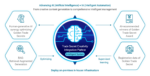
Trade Secret Sustainable Intelligent Management Center
Also Read:
TSMC Powers Up: 408,000 Batteries Get a Safety Intelligence Upgrade
Siemens EDA Expands AI and Advanced Packaging Collaboration with TSMC
imec IC-Link and TSMC 3DFabric Alliance Expansion Signals New Era of System-Level Scaling