Semiconductor fabs aim to have high yields and provide processes that attract design firms and win new design starts, but how does a fab deliver their process nodes in a timely manner without having to run lots of expensive silicon through the line? This is where simulation and TCAD tools come into play, and to learn more about this field I attended a Silvaco webinar. Mao Li from Silvaco presented the webinar and had over 50 slides to cover in under 45 minutes, so it was fast-paced.
Silvaco offers TCAD tools for accurate 3D simulation and device optimization, applicable to processes spanning CMOS, memory, RF and power devices. Logic CMOS technology in the past 20 years has gone from 90nm to the Angstrom era, using planar, FinFET, GAA and 3D structures, like CFET. Each generation of fab technology has presented unique technical challenges that required new modeling capabilities for simulation in TCAD tools.
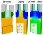
Mr. Li talked about stress and HKMG (High-K Metal Gate) process challenges that required both 2D and 3D simulation approaches. FinFET technology required new transistor-level process simulation for structure, doping and stress effects, this is where Victory Process is used.
Following process simulation comes device simulation, where the transistor characteristics are predicted for NFET and PFET devices using Victory Device.
Going beyond individual transistors, they can simulate standard cell layouts in their 3D structure, followed by parasitic extractions with Victory RCx to enable the most accurate SPICE circuit simulations. Silvaco showed their flow from TCAD to SPICE, enabling Design Technology Co-Optimization (DTCO).
Memory technology was presented, starting with the history of DRAM evolution, and the pursuit of ever-smaller cell sizes. 3D modeling of saddle fin shapes is supported for DRAM cell arrays.
3D NAND process integration was explained using two engines, Victory Cell mode using an explicit mesh and Victory Process mode using a level set. Stress simulation for 3D NAND results were presented, along with the cell device electrical characteristics.
High-frequency and high-performance applications like wireless communications, radar, satellite and space communications use RF-SOI process technology, and this is modeled and simulated with the Victory tools. High-voltage power devices in LDMOS technology were accurately modeled using 2D or 3D techniques.
The big picture from Silvaco is that their tools are used by both simulation and fab engineers to enable Fab Technology Co-Optimization (FTCO), from automating Design of Experiments using modeling of process, device and circuits, all the way to building a Digital Twin for fab engineers.
For process simulation each step is modeled: etch/deposit, implantation, diffusion and activation, stress. Device simulation includes both a basic model and advanced model. Parasitic extraction uses a 3D structure, then applies a field solver for most accurate RC values. The Victory Process tool is continually improved to include two new diffusion models for best accuracy, especially for 3D FinFET devices. These models are extensively calibrated across doping species, implantation dose ranges, temperature ranges and annealing time ranges.
Development continues for advanced structure generation, along with speed ups in runtime performance. Support of orientation of the silicon lattice has been added, plus new quantization models, and advanced mobility effects.
Instead of using trial and error fab runs to develop a process, using this AI-driven FTCO approach will save engineering time, effort and costs. A case study for FinFET device performance was shared that used machine learning from the Victory DoE and Victory Analytics tools, allowing users to find the optimal input values to satisfy multiple outputs. MonteCarlo simulation was used for both margin analysis and Cp/Cpk characterization.
Summary
Silvaco has a long history in TCAD tools and over time their products have been updated to support fab processes across CMOS, memory, RF and Power devices. Using TCAD for 3D silicon simulation is a proven approach to save time to market. FTCO is really happening.
View the webinar recording online for more details.
Related Blogs