In the race to deliver ever-larger SoCs under shrinking schedules, simulation is becoming a bottleneck. With debug cycles constrained by long iteration times—even for minor code changes—teams are finding traditional flows too rigid and slow. The problem is further magnified in continuous integration and continuous deployment (CI/CD) environments, where each commit may trigger a full simulation cycle, consuming unnecessary time and compute resources. Siemens EDA’s SmartCompile aims to break this logjam.
SmartCompile: A Paradigm Shift in Simulation Workflows
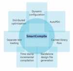
Siemens EDA addresses this critical challenge with SmartCompile, a feature of its Questa One simulation environment. Rather than iterating on top of the traditional flow, SmartCompile introduces a fundamental redesign of the compile-optimize-simulate pipeline. It adopts a modular and highly parallel approach to managing design verification tasks, enabling faster turnaround times without compromising design integrity.
The foundation of SmartCompile’s innovation lies in its ability to break apart large, monolithic processes into discrete, manageable units. This divide-and-conquer philosophy allows each component—be it compilation, optimization, or test loading—to be performed independently and in parallel, dramatically improving simulation readiness and design iteration velocity.
Enhancing Performance through Incremental Workflows
One of the most significant advantages of SmartCompile is its incremental compilation and optimization strategy. By utilizing timestamp tracking and smart signature analysis, the system identifies precisely which parts of the design have changed and compiles only those. This targeted approach drastically reduces build times across repeated verification cycles and streamlines test and debug cycles for developers.
Furthermore, the introduction of separate test loading revolutionizes how simulation teams manage test scenarios. Instead of recompiling the entire testbench for each new test, SmartCompile allows users to reuse the base compilation and optimization while isolating and processing only the new or modified tests. This capability significantly accelerates the test development process and promotes faster feedback loops during debugging.
Tackling Design Scale with Intelligent Partitioning
As designs increase in complexity, optimization becomes one of the most time-consuming stages of verification. To combat this, SmartCompile introduces the concept of AutoPDU—automatically pre-optimized design units. This feature partitions large designs into smaller, manageable units that can be independently compiled and optimized. When changes are made, only the affected units need to be processed again, leaving the rest untouched. This approach not only reduces the time required for each optimization run but also allows the process to be distributed across multiple grid computing nodes. By enabling parallelism at the design unit level, AutoPDU transforms how large SoCs are handled, dramatically decreasing overall simulation setup time.
Boosting CI/CD Efficiency with SmartCompile
Questa One’s SmartCompile is uniquely suited to enhance CI/CD (Continuous Integration and Continuous Deployment) pipelines in hardware design. By enabling rapid, incremental builds and leveraging precompiled design caches, SmartCompile allows frequent code check-ins to be verified quickly without reprocessing the entire design. Its intelligent reuse of elaboration and optimization data significantly reduces turnaround times in automated workflows. This capability ensures that regression tests, triggered automatically by CI systems, execute efficiently, allowing development teams to scale their productivity while maintaining robust quality assurance throughout the design lifecycle. This feature is particularly valuable for large teams and distributed projects, where multiple engineers may need to reproduce simulation environments “on demand—without losing valuable time.”
Flexible Configuration for Advanced Use Cases
In many simulation environments, different abstraction levels—such as RTL, gate-level, or behavioral models—are needed for different verification tasks. Traditionally, switching between these configurations requires recompilation and re-optimization. SmartCompile’s dynamic reconfiguration capability removes this barrier by allowing blocks to be swapped in or out at simulation time. This feature lets users pre-compile various block configurations and select the appropriate one during elaboration, enabling greater flexibility and reducing redundant processing.
Additionally, debug data generation in SmartCompile is no longer tightly coupled with optimization. Engineers can generate debug files on demand, rather than each time a build is processed. This not only improves resource efficiency but also empowers teams to target their debugging efforts more precisely.
The Business Value of Smarter Simulation
The cumulative effect of these innovations is substantial. SmartCompile enables design teams to iterate faster, simulate more often, and reduce wasted compute cycles. With its support for incremental workflows, distributed optimization, configuration flexibility, and CI-friendly features, it presents a compelling solution for organizations looking to scale their design verification capabilities without scaling their costs. This means faster time-to-market, reduced operational expenses, and more reliable development pipelines. As competition in the semiconductor market intensifies, the ability to verify designs quickly and efficiently becomes a critical differentiator. By integrating SmartCompile into their verification strategy, companies can better manage complexity while maintaining agility and performance.
Summary
Simulation has always been a cornerstone of digital design verification, but as designs grow more complex and development timelines shrink, traditional flows no longer meet the needs of modern engineering teams. Siemens EDA has recognized this shift and responded with a comprehensive and intelligent approach in SmartCompile. It tackles the fundamental inefficiencies of traditional workflows, enabling faster, smarter, and more scalable verification from the ground up.
Also Read:
Siemens EDA Unveils Groundbreaking Tools to Simplify 3D IC Design and Analysis
Jitter: The Overlooked PDN Quality Metric
DAC News – A New Era of Electronic Design Begins with Siemens EDA AI