RVN! 26 Banner revised (800 x 100 px) (600 x 100 px)

Static Timing Analysis Signoff – A comprehensive and Robust Approach

Static Timing Analysis Signoff – A comprehensive and Robust Approach
by Admin on 09-02-2025 at 6:00 am

pic2 xtalk circuit

By Zameer Mohammed

Once a chip is taped out, changes in design are not possible – Silicon is unforgiving, does not allow postproduction modifications. In contrast, software can be updated after release, but chips remain fixed. Static Timing Analysis (STA) signoff serves as a crucial safeguard against silicon failures.

In modern VLSI design, errors are extremely costly, impacting finances, time-to-market, product credibility, and safety for critical applications. Missing just one STA check can result in multimillion-dollar losses and significant project delays.

“Only Paranoids Survive – a cautious and thorough approach is essential for STA signoff”

Objectives of a good STA Signoff Methodology
  • Comprehensive set of signoff checks – every detail examined

STA signoff checks are required to meet the specifications established by technology, design, project, and blocks. These signoff checks must identify structural issues, verity correct STA execution, perform all mandated timing analyses, and incorporate any custom checks relevant to the specific node or design.

  • Ensure flawless signoff without errors or omissions

Conducting a comprehensive review of signoff specifications and code implementations, coupled with the integration of automated processes and log parsing for all signoff output logs and reports, alongside the proper application of waivers and effective communication regarding un-waived signoff violations, is critical for ensuring robust STA Signoff quality.

  • Find pessimism in signoff specifications and extreme constraints

The STA signoff process should efficiently identify unrealistic constraints and provide robust debugging reports. Structuring reports by violation type, severity, design, and operating mode – supported by clear charts and statistical summaries such as frequency histograms – significantly improve clarity. Additionally, early identification of inflated requirements is essential to ensure effective STA signoff.

  • Early timing closure feedback to resolve issues proactively

Prioritizing essential signoff checks that could lead to future bottlenecks, along with providing clear feedback, debug data, and proposed solutions, help achieve a faster Timing Closure cycle.

Key Attributes of STA Signoff Methodology

 While it’s beyond the scope of this article to go over detailed algorithm of each of the STA signoff checks, a single signoff check is presented here with details.

Crosstalk on Nets – Custom STA Signoff Check Crosstalk

Crosstalk complicates timing closure by causing pattern-dependent and corner-sensitive delay variation that can break both setup and hold times. It introduces noise that may lead to the glitches, false captures, and increased jitter, reducing overall design margins. Crosstalk also negates CPPR credit and negatively affects both capture and launch for the same timing path due to worst case analysis. Block to top miscorrelation is also attributed to crosstalk on boundary nets. This could force costly ECOs involving re-routing, shielding with potential ripple effects on power, DRC and EMI closure.

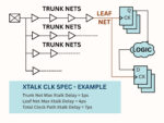
It is important to set crosstalk limits for datapath, clock trunk and clock leaf nets, and to verify each net in design. An example is presented below with details.

Trunk Nets are generally targeted to have zero crosstalk delay component, as excessive crosstalk can complicate timing closure. Common methods of crosstalk mitigation include double spacing and shielding. On critical routes, differential clock routing maybe employed. In practice, some nets may not meet this target, so establishing a conservative and reasonable crosstalk limit is recommended. The goal is to maintain a crosstalk clean clock trunk network.  Because each path can involve large number of nets, it’s vital to keep the clock trunk network free of crosstalk, as it accumulates along the path.

Leaf Nets cannot be shielded or isolated since they represent the final stage of clock network and are connected to an equal number of sequential devices making shielding and isolation (by double or triple spacing) resource intensive. Consequently, it is generally acceptable to allow 4-5 ps of crosstalk on each leaf net. To manage potential issues, a cumulative limit can be established for total crosstalk along the nets in clock path, enabling oversight of both excessive crosstalk on individual leaf nets and combined effect from the trunk and leaf net crosstalk.

A structured approach involves analyzing 1000 paths per clock domain for example, collecting all nets pertaining to the capture clock path, and extracting delays associated with cross coupling effects. Constructing a frequency distribution table with crosstalk delay intervals ranging from 1ps to 10 ps facilitates assessment of the clock network’s performance in relation to cross coupling. Additionally, performing this signoff verification and comparing results consistently provides an early indication of any clock network degradation. Prompt identification of issues as they arise is essential for effective Timing Closure.

Categorized “STA Signoff” checks & description

The list of STA signoff checks is very comprehensive, with at least 50 signoff checks; here are the key ones with brief description. Detailed coverage of all checks is outside the scope of this article.

  • STA Signoff Spec Implementation Check First Signoff Step

STA Margins – Verify margins and guard bands applied for each relevant check, whether tool-generated or user-defined.

Timing Derates – Check Process, Voltage, Temperature, Aging, Radiation, MixVT and distance based derates for design /cell /net / constraints / checkTypes.

Clock Uncertainties – Check clock uncertainty specification based on clock period percentages or a flat number for each clock or design.

Full Cycle Jitter – Measure Jitter, modeled as additional clock uncertainty and usually specified as compounded root mean square sum of PLL jitter and CTS network jitter.

Half Cycle Jitter – Similar to full cycle jitter, measure jitter applied to half cycle paths and min pulse width checks.

Input Drive – Check for presence of driving cell and confirm either the default or custom driver for each port based on PVT conditions during timing analysis.

Output Load – Verify the default minimum load, and custom loads based on presence of I/O pads or special external specifications for output drivers.

STA Flow Variables – Hundreds of variables steer accurate signoff STA, requirements dictated by tool version, technology node or foundry specification, project intent, STA methodology and signoff specification.

STA Command Options – Same details as STA Flow Variables applies to options used in Commands to execute STA steps.

STA Corners – Check to ensure signoff spec matches the STA corners for which analyses is performed. (PVTRC x Functional/Scan/JTAG/CDC …)

Max Transition Limits – Verify that max transition reports reflect minimum library constraints and any over constraint on clock domains or designs set by project/design to achieve superior timing performance.

Max Cap Limits – Same details as Max Transition Limits apply to Max Capacitance checks. Usually, library defaults used for internal nodes.

Asynchronous Clock Groups – Collect timing paths with finite slack from all clock group combinations, and trace master and generated clocks to determine clock crossings from reported paths that are not part of same family.

  • Input Acceptance CriteriaPreventing Junk In Junk Out scenario Netlist Quality – Confirm accurate read design process and check for any netlist structure or hierarchy binding errors or warnings.

Timing Constraints Quality – Ensure accurate reading of constraints files, free from unwaivable errors and warnings, confirm the correctness of master and generated clock definitions, and verify the proper implementation of timing exceptions.

Annotation Parasitics Quality – Check correct read of parasitic annotation files, audit extraction logs for signoff (layers, flow variables, log parse of extraction files, correct tech file usage, inclusion of metal fill, location information in parasitics if applicable).

Design Library Usage Correctness – Verify correct library usage for standard cells, io pads, memories, custom IPs from various choices within released library database.

Tool Versions Correctness – Correct tool versions for timing, extraction, constraint generation, IP model generation & Unix usage (csh, python, lsf/bsub…)

File Versions – Check correct versions of files for Variation (POCV/SOCV), Power Configuration (UPF), Netlists (.vg, .libs), Parasitics (SPEF), STA Flow Versions.

  • Structural ChecksSignificant flaws in design construction, backup STA checks Don’t Use Cells – Clock & Data don’t use cells as per foundry, project and block spec based on cell type, cell strength and placement in timing path.

Must Use Cells – Clock & Data cell types (flop types, clock buffers, i/o drivers …)

Synchronizer Cell Types – Check specific allowable pattern for stage1 and stage2 synchronizers (library cell, strength, vt type)

Synchronizer Cell Proximity – Check to ensure 2 stages of synchronizers abut with each other or placed right next to each other for optimal metastability failure times.

Synchronizer Cells Structure – Check to ensure only net and no cell exists in between 2 stages of synchronizers.

Delay Cells & Structure – Check to ensure right delay cell type and strength, and maximum number of allowable contiguous delay cells in a timing path, to ensure no optimism in delay cell variation modeling.

Lockup Latch Structure Correctness – Half cycle path lockup latch capture polarity correctness (can’t rely on external tools), lockup latch cell type and placement of lockup latch close to launch clock (destination can absorb clock skew not source)

Sparecell Density – Check sparecell density spec per block.

Port Fanout – Ensure single fanout of all critical data or clock ports to avoid overload in upper-level instantiations, and to ensure block/top correlation related to spatial derates bounding box.

Input Port Net Length – Ensure optimal net load when modules are multiply instantiated at higher levels.

Timing Path Depth – Every clock domain examined for critical path depth, a finite limit must be ensured for low risk down the timing closure phases, also an early indicator of timing convergence risks if done pre-layout STA.

Power Management Cell Structure – Cell type and correct instantiation of isolators, level shifters, enable level shifters, voltage interface cells, retention flops, retention memories, power switches, reset isolation cells, always on buffers, clamp cells & bus hold cells.

VT Type Usage – Percentage usage of various VT flavors as per spec for each block and chip overall usage.

MixVT Usage – VT spec is based on single VT usage for clock or datapath. If MixVT is used, additional VT penalty must be applied. Check is necessary to detect MixVT and fix structure of design, or apply additional margins/derates.

  • STA Run Correctness ChecksSignoff Process Validity

Design Linking – Check to see if all designs linked, any port mismatches, empty modules, black boxes etc. Crucial to make sure every design element is timed, and every single timing arc is covered without going into analysis coverage debug.

Parasitic Annotation Coverage – Ensure all nets annotated with Resistance, Ground Capacitance and Coupling Capacitance, also checked for floating/dangling nets.

Correct Spef Transformation – When multiple SPEFs stitched at higher levels, correct orientation and block size must be read in via PDEF or custom commands, for correct distance calculations used in distance based derates. Also, can’t trust any tool with correct calculation even though tools handle design origin and orientation automatically. This check is very crucial to also cover issues like not reading such location details from SPEF files etc.

Constraints Analysis Coverage & Quality – Unclocked sequential cells and untimed timing endpoints in the context of STA analysis mode are two most critical coverage items for every STA check. Additionally conflicts in case analysis, ignored exceptions, master clock non propagation to generated clocks, any constraints non propagation.

Derates & Margins Coverage – Check derates application for cell, net, constraints (setup, hold, min pulse width) related to Process, Voltage, Temperature, Aging, Radiation, mix VT usage. Also check guard bands or margins for pre-layout, block specific or additional signoff pessimism.

Log Parsing -Most important signoff step, every error or warning must be flagged, reviewed, waivers validated and closed before a thumbs up for tapeout or STA signoff. This must be run with every block, every regression of STA in automated mechanism. No Excuses.

PBA/GBA Convergence – Most PD tools and STA under the hood run GBA and then perform PBA analysis with GBA baseline. 100% coverage for PBA is achieved by various custom algorithms. When tools can’t converge, they fall back to GBA timing on those specific paths and issue messages about non convergence.  Checks must be done to ensure 100% PBA GBA convergence to remove pessimism is timing (which is not harmful, but not accurate and time consuming to close on GBA timing)

STA Units Correctness – SDC time units, Capacitance units, Resistance units – SDC unit are specified in sdc, decoded from library read or set in STA flow. Each tool has difference precedence rules to interpret units. And correct usage is essential to interpret SDC. Reporting units are different from library units. Library units handled by tool whereas reporting units help STA users interpret reports with consistency and known formats.

STA View Completeness – Check to make sure all functional and scan modes, and all PVTRC analysis corners have been analyzed based on project specification.

STA Run Completeness – Based on all STA views executed, make sure each run ended correctly, all phases of STA executed, and job status from Unix/LSF/BSUB had no unexpected termination, any issues in STA due to disk failures, TMP space, additional license availability etc.

  • STA Metrics ChecksThe real STA checks for signoff Standard Timing Path Checks – Setup, Hold, Recovery, Removal, Clock Gating, Data to Data Checks.

Design Rule Checks – Max Transition(slew), Max Capacitance, Max Fanout

Special Checks – Min Period/Clock Period, Min Pulse Width, Noise, Double Clocking.

  • STA Custom ChecksAdditional robustness check for high quality STA signoff

Max Clock Skew – Skew is never a criterion to signoff as its impact is already absorbed in various timing violations, but excessive skew can expose variation modeling flaws and can cause silicon failures, it’s a good practice to have reasonable limit on skew in any path.

Excessive Xtalk – Crucial component of timing closures, hurts both setup/hold simultaneously, lethal for checks like Min Pulse Width. Exacerbates block to top correlation, impacts Common Path Pessimism Removal (CPPR) credit and impacts cell/net delays in any path. Proper limits must be set in terms of coupling cap or delays or transition times for coupled nets for datapath and clocks.

Dynamic Jitter Validation – For each clock domain, calculate dynamic jitter by compounding source PLL jitter with CTS network jitter (root mean square of each stage element CTS network jitter) and validate against per clock domain jitter spec. Used only in high performance designs where we its very conservative to apply flat jitter number to all clocks or groups of clocks.

Half Cycle Paths – Custom timing reports to analyze half cycle paths as they have half cycle jitter and custom uncertainties and margins, IP interfaces, scan paths etc.

And the list is endless – Based on technology node, company STA philosophy, signoff owner paranoia, sky is the limit to custom STA checks.

Failure to implement the STA signoff methodology outlined above will lead to frequent bugs, negatively affect Time to Market, incur expensive design fix cycles, and diminish the credibility of the signoff process, which is the most critical factor.

Zameer Mohammed

Zameer Mohammed is a timing closure and signoff expert with over 25 years of experience, having held key technical lead roles at Cadence Design Systems, Apple Inc., Marvell Semiconductor, Intel, and Level One Communications. He specializes in STA signoff for complex ASICs, with deep expertise in constraints development and validation, synthesis, clock planning, and clock tree analysis. Zameer holds an M.S. in Electrical Engineering (VLSI Design) from Arizona State University and is a co-inventor on U.S. Patent No. 9,488,692 for his work at Apple.

Also Read:

Orchestrating IC verification: Harmonize complexity for faster time-to-market

Perforce and Siemens at #62DAC

Synopsys Enables AI Advances with UALink


Beyond Traditional OOO: A Time-Based, Slice-Based Approach to High-Performance RISC-V CPUs

Beyond Traditional OOO: A Time-Based, Slice-Based Approach to High-Performance RISC-V CPUs
by Kalar Rajendiran on 09-01-2025 at 10:00 am

Hot Chips Logo 2025

For decades, high-performance CPU design has been dominated by traditional out-of-order (OOO) execution architectures. Giants like Intel, Arm, and AMD have refined this approach into an industry standard—balancing performance and complexity through increasingly sophisticated schedulers, speculation, and runtime logic. Yet, as workloads diversify across datacenter, mobile, and automotive domains, the weaknesses of conventional OOO architectures—power inefficiency, complexity, and inflexibility—are becoming more pronounced.

Now, a new paradigm is emerging: Time-Based OOO microarchitecture. Anchored in both research and new patents, this approach offers a disruptive alternative that may give RISC-V its first defensible high-performance edge against entrenched incumbents. In the RISC-V era, where openness, extensibility, and ecosystem leverage are key differentiators, time-based OOO provides a path to leapfrog legacy incumbents.

At Hot Chips 2025, Ty Garibay and Shashank Nemawarkar from Condor Computing gave a talk on this topic. They presented details of their processor architecture (code name: Cuzco), a high-performance, RVA23 compatible RISC-V CPU IP, featuring a time-based OOO execution and a slice-based microarchitecture. Ty is the company’s President and Founder and Shashank is a Senior Fellow and the Director of Architecture.

The Key Idea: Time as a First-Class Resource

Traditional OOO processors rely on per-cycle schedulers that dynamically resolve dependencies and issue instructions. While effective, this method requires large, power-hungry hardware structures—reservation stations, wakeup/select logic, and dynamic scoreboard tracking—that scale poorly with wider, superscalar cores.

Time-based OOO execution flips this model. A Register Scoreboard tracks the future “write time” of instructions, so that downstream instructions automatically know when operands will be ready. A Time Resource Matrix (TRM) records busy intervals for execution resources such as ALUs, buses, load/store queues, which helps predict resource availability cycles ahead of time. This enables predictive scheduling, where instructions are issued with knowledge of exact future cycles for operands and resources.

In practice, this transforms instruction scheduling into something akin to a compiler’s static analysis, but executed in hardware with runtime adjustments for mispredicts, cache misses, and dynamic latencies. This results in lower gate count, reduced dynamic power, and simpler logic—while still delivering high IPC performance.

Why Now? Closing the Tooling and Ecosystem Gap

The concept of time-based scheduling is not new in academic research—but several barriers prevented its adoption in industry:

Historically, CPU design relied on proprietary, closed toolchains and performance modeling frameworks. Implementing a radically different scheduling model required deep compiler and simulator co-design—an almost impossible ask without community-driven support. The rise of RISC-V changes the equation. Open-source modeling frameworks like Sparta, Olympia, Spike, and Dromajo provide extensible platforms for exploring new scheduling strategies. Condor Computing has contributed new tools, such as Fusion Spec Language (FSL), and actively contributed toward Dromajo and Spike enhancements, to enable precise modeling and ecosystem-wide adoption. Where traditional OOO once benefited from standardization and inertia, the high performance RISC-V OOO now benefits from open-source leverage and community contributions. Time-based OOO rides on plug-and-play comparisons and refinements over traditional OOO techniques using these tools.

Cuzco’s Slice-Based Design: Flexible, Efficient and Scalable

Slice-based microarchitecture delivers scalability, efficiency, and flexibility by breaking a CPU into modular, repeatable “slices,” each with its own pipelines and resources. This approach avoids the critical-path bottlenecks of monolithic superscalar designs, enabling predictable performance scaling from low-power IoT to datacenter workloads. Customers achieve static configurability by choosing two, three or four slices depending on their area/power/performance requirements. They can also achieve dynamic configurability by power-gating slices at runtime, allowing the processor to scale down for lower-power workloads. The result is higher performance-per-watt, faster time-to-market, and a more flexible IP offering that customers can tailor to diverse use cases.

Customer Benefits

For customers evaluating licensable CPU IP, the appeal of time-based OOO is not only architectural elegance but also tangible benefits:

  • Performance-per-Watt: Comparable or superior IPC to traditional OOO
  • Scalability: Supports up to 8 cores per cluster with private L2 and shared L3 caches, delivering datacenter-grade throughput without prohibitive power budgets.
  • Predictability: Simplified scheduling reduces verification complexity and gate count, speeding up time-to-market compared to traditional OOO designs.
  • Customization: Native RISC-V ISA extensibility, combined with TRM-driven scheduling, enables faster deployment of domain-specific accelerators—critical for AI, networking, and automotive use cases.

Summary

Cuzco’s time-based out-of-order execution represents a fundamental rethinking of CPU design. By eliminating the inefficiencies of per-cycle scheduling, it reduces complexity, lowers power, and enables broader scalability—all while remaining fully compatible with the RISC-V ISA and software ecosystem.

It’s a RVA23 compatible processor that delivers the best performance per watt and per sq.mm in licensable CPU IP. This is not an incremental improvement but rather a structural shift that could define the high-performance era of RISC-V.

Cuzco is designed for broad applicability:

  • Datacenters: High throughput with lower power budgets translates to lower TCO.
  • Mobile & Handsets: Energy efficiency with competitive performance.
  • Automotive: Predictability and determinism, critical for safety workloads.
  • Custom Accelerators: Domain-specific optimizations unlocked by RISC-V ISA extensibility.

To learn more:

Contact Condor Computing at condor-riscv@andestech.com

Visit Andes Technology website.

Visit Condor Computing website.

You can access this talk, on-demand from here. [Link once Hot Chips provides the link for general access]

Also Read:

Andes Technology: Powering the Full Spectrum – from Embedded Control to AI and Beyond

Andes Technology: A RISC-V Powerhouse Driving Innovation in CPU IP

Andes RISC-V CON in Silicon Valley Overview


eBook on Mastering AI Chip Complexity: Pathways to First-Pass Silicon Success

eBook on Mastering AI Chip Complexity: Pathways to First-Pass Silicon Success
by Admin on 09-01-2025 at 8:00 am

MArtering AI Chip Complexity Synopsys

The rapid evolution of artificial intelligence (AI) is transforming industries, from autonomous vehicles to data centers, demanding unprecedented computational power and efficiency. As highlighted in Synopsys’ guide, the global AI chip market is projected to reach $383 billion by 2032, growing at a 38% CAGR. This surge is driven by AI models scaling to trillions of parameters, outpacing traditional monolithic chips. To meet these demands, the industry is shifting toward chiplet-based and multi-die designs, enabling scalability, heterogeneous integration, and optimized performance. However, this transition introduces formidable challenges: silicon complexity reaching hundreds of billions of transistors, shrinking design cycles to 12 months, soaring costs exceeding hundreds of millions per chip, and acute talent shortages. At least 58% of ASICs require respins due to logic flaws, underscoring the need for a holistic approach to achieve first-pass success.

Central to mastering these complexities is early architecture exploration. Designers must address performance, power, and cost trade-offs upfront, using tools like Synopsys’ Platform Architect for monolithic and multi-die modeling. This “shift-left” methodology optimizes CPU configurations, memory hierarchies, and interconnects, such as UCIe for die-to-die links and PCIe 7.0 for high-speed interfaces. By simulating AI workloads early, teams can reduce schedule risks by 3-6 months, ensuring efficient data movement and energy use. Power optimization is paramount, as data centers could consume 1,000 TWh by 2026—equivalent to entire nations’ energy needs. Integrating real-world workloads prevents bottlenecks in memory bandwidth and thermal management.

Silicon front-end and back-end design further amplify these efforts. RTL design demands excellence to avoid costly respins, with Synopsys’ integrated flows leveraging AI-driven verification for seamless simulation across chiplets. Back-end tools like Fusion Compiler enable hyper-convergent workflows, balancing power-performance-area (PPA) while handling high-density HBM and UCIe interfaces. Cloud-based solutions, such as Synopsys Cloud and ZeBu Cloud, provide on-demand scalability, eliminating CapEx barriers for startups and managing peak demands for enterprises. This is exemplified by Rain AI, which accelerated innovation using Synopsys’ suite, focusing on power-efficient compute engines.

Advanced packaging and multi-die design break reticle limits, but introduce issues like signal integrity and system pathfinding. Synopsys’ 3DIC Compiler, in collaboration with Ansys, offers end-to-end solutions for thermal and power-aware co-design, supporting UCIe standards and foundry partnerships with TSMC and Intel. Early software development parallels hardware via virtual prototypes and hardware-assisted verification (HAV), allowing quadrillions of cycles for validation. NVIDIA’s adoption of HAPS-200 prototypes achieved 50 MHz speeds, boosting software productivity in compressed cycles.

Security considerations are non-negotiable, with AI threats like data poisoning and model theft. Synopsys provides certified IP for root-of-trust, secure interfaces, and post-quantum cryptography, safeguarding multi-die systems. Finally, Silicon Lifecycle Management (SLM) ensures long-term reliability through in-field monitoring, RAS features, and predictive analytics, as seen in AWS Trainium deployments.

Bottom line: Synopsys turns AI chip challenges into opportunities by offering comprehensive EDA tools, IP, and ecosystem collaborations. By parallelizing design tracks and emphasizing early optimization, innovators can achieve resilient, high-performance silicon. As AI reshapes the world, partnering with Synopsys ensures first-pass success, driving innovation from concept to deployment.

Get the full eBook here.

About Synopsys

Synopsys, Inc. (Nasdaq: SNPS) is the leader in engineering solutions from silicon to systems, enabling customers to rapidly innovate AI-powered products. We deliver industry-leading silicon design, IP, simulation and analysis solutions, and design services. We partner closely with our customers across a wide range of industries to maximize their R&D capability and productivity, powering innovation today that ignites the ingenuity of tomorrow. Learn more at www.synopsys.com.

Also Read:


Orchestrating IC verification: Harmonize complexity for faster time-to-market

Orchestrating IC verification: Harmonize complexity for faster time-to-market
by Admin on 09-01-2025 at 6:00 am

fig1 optimize ic with mjs

By Marko Suominen and Slava Zhuchenya of Siemens Digital Industries Software.

It’s often said that an orchestra without a conductor is just a collection of talented individuals making noise. The conductor’s role is to transform that potential cacophony into a unified, beautiful symphony. The same concept holds for complex integrated circuit (IC) verification.

The sheer scale and intricacy of modern chips present a formidable orchestration challenge to verification teams. It’s no longer just about running individual design rule checks (DRC) or layout versus schematic (LVS) runs; it’s about managing an entire symphony of verification tasks, often playing out across different teams, tools and timelines.

This escalating complexity has exposed a critical bottleneck: the lack of a cohesive, automated system to manage the entire verification workflow. Without a conductor for this intricate orchestra, teams often find themselves mired in manual coordination, resource contention and the constant risk of missed steps, all of which directly impact crucial time-to-market windows.

Chaos: The unorchestrated verification flow

Imagine a verification environment where each type of check—DRC, LVS, parasitic extraction, electrical rule checks (ERC), and more—is initiated and monitored in isolation. Design IPs arrive from various sources, each with subtle differences in conventions like text labels or bus bit separators. Engineers must manually track dependencies, prioritize jobs, and ensure that all necessary runs are completed in the correct sequence.

This fragmented approach leads to several pervasive challenges:

  • Scale limitations: As designs grow, so does the volume of verification data. Manually managing thousands or even millions of violations, or processing results from dozens of individual runs, becomes overwhelming and error-prone.
  • Context fragmentation: Without a unified view, engineers struggle to see the holistic picture of the verification process. Issues are addressed in silos, making it difficult to identify systematic problems or optimize the overall flow.
  • Tedious manual management: The administrative burden on engineers is immense. Submitting jobs, checking statuses, managing licenses, and coordinating with other teams consumes valuable time that could be spent on actual design and debug.
  • Inefficient resource utilization: Compute resources and expensive EDA tool licenses may sit idle or become bottlenecks due to uncoordinated job submissions, leading to suboptimal throughput and increased operational costs.
  • Risk of missed steps: Human error is inevitable. In a manual environment, it’s easy for a critical check to be overlooked, a dependency to be mismanaged, or a run to be forgotten, leading to costly reruns or, worse, undetected design errors that surface late in the cycle.

These challenges highlight a fundamental truth: the efficiency of modern IC design is increasingly dependent on the efficiency of its verification workflow.

The rise of verification orchestration: A conductor for complexity

To overcome these hurdles, the industry is increasingly recognizing the need for dedicated verification workflow management or job orchestration solutions. These systems act as the central conductor, bringing order, automation, and predictability to the complex verification process.

A robust verification orchestration system typically offers:

  • Unified control and monitoring: A single graphical user interface (GUI) provides a comprehensive view of all verification jobs, their status, and dependencies. This eliminates the need to jump between multiple tools or windows.
  • Automated flow capture and execution: The ability to define and store entire verification flows as templates ensures that all necessary checks and tasks are included. Users can initiate complex sequences of jobs—sequential or parallel—with a single click, drastically reducing manual effort and the risk of human error.
  • Intelligent resource management: Such systems can optimize the use of compute resources and licenses. Features like license queuing ensure that licenses are allocated efficiently, and the ability to stream out layout data once for multiple runs significantly reduces redundant I/O operations and overall runtime.
  • Enhanced visibility and notifications: Centralized status monitoring and automated notifications (e.g., email alerts upon job completion) free engineers from constant manual checking, allowing them to focus on analysis and debug.
  • Improved collaboration: By providing a consistent, shared view of the verification status and results, these systems foster better communication and collaboration across design and CAD teams.

For instance, the Calibre Interactive Multiple Job Submission (MJS) GUI (Figure 1) is one such solution that exemplifies these capabilities. It allows design teams to intuitively manage and monitor all their verification jobs from a single interface, capturing entire sign-off flows into a single “Jobs Setup” file. This templated approach ensures that every aspect of the verification process is thoroughly accounted for, mitigating the risk of missed runs or checks.

Figure 1. The Calibre MJS GUI with multiple verification jobs submitted. Monitor all the jobs from one place.

Real-world impact: Streamlining verification for leading innovators

The practical benefits of adopting a verification orchestration approach are significant. A leading telecommunications company, for example, transformed its IC design verification workflows by adopting the Siemens Calibre MJS system. They experienced substantial improvements in automation, resource management and operational efficiency.

For top-level designers, the ability to automate and capture the entire verification flow meant eliminating manual initiation of multiple runs and reducing human error. Features like streamlined layout streaming (where the layout is streamed out only once for all runs) and efficient license usage (through license queuing and flexible allocation) directly contributed to faster throughput and optimized costs.

At the block level, the system provided a templated approach to physical verification (PV) flows, ensuring that no essential steps were overlooked. This “all-in-one” sign-off capability allowed designers to run all possible PV flows within a single platform, simplifying job submission and facilitating rapid iterations during design fixes.

The imperative of orchestration

As IC designs continue their trajectory of increasing complexity, the traditional, fragmented approach to verification is no longer sustainable. The ability to orchestrate the entire verification workflow, from individual checks to comprehensive sign-off, is becoming a non-negotiable requirement for competitive advantage.

By embracing a dedicated verification workflow management solution, design teams can move beyond manual overhead and reactive debugging. They can achieve greater efficiency, reduce the risk of costly errors, optimize valuable resources, and ultimately, accelerate their time-to-market. In the symphony of modern IC design, a capable conductor for verification is no longer a luxury, but an essential component for success.

Marko Suominen is a Calibre application engineer in Siemens Digital Industries Software and based in Helsinki, Finland. He helps his customers in the central and northern Europe to make successful IC design projects with Calibre products including more recent tools like Calibre 3D Thermal and Insight Analyzer. He received M.S in electrical engineering from Helsinki University of Technology (currently known as Aalto University). He could be reached at marko.suominen@siemens.com.

Slava Zhuchenya is a product engineer supporting Calibre interface tools in the Design-to-Silicon division of Siemens Digital Industries Software. His primary focus is the support and enhancement of the Calibre RVE and Calibre Interactive products. Previously, Slava was a member of the Calibre PERC R&D team. He received a B.S. in electrical engineering from Portland State University. Slava may be reached at slava_zhuchenya@siemens.com.

Also Read:

Breaking out of the ivory tower: 3D IC thermal analysis for all

Software-defined Systems at #62DAC

DAC TechTalk – A Siemens and NVIDIA Perspective on Unlocking the Power of AI in EDA


Basilisk at Hot Chips 2025 Presented Ominous Challenge to IP/EDA Status Quo

Basilisk at Hot Chips 2025 Presented Ominous Challenge to IP/EDA Status Quo
by Jonah McLeod on 08-31-2025 at 10:00 am

Hot Chips Logo 2025

At Hot Chips 2025, Philippe Sauter of ETH Zürich presented Basilisk, a project that may redefine what’s possible with open-source hardware. Basilisk is a 34 mm² RISC-V SoC fabricated at IHP Microelectronics on its open-source 130nm BiCMOS process in Germany. Basilisk, named after the Greco-Roman mythical creature known for its lethal gaze, runs full Linux and, more importantly, was produced entirely with open-source EDA tools. The achievement goes beyond a one-off demo. By proving that a Linux-capable SoC can be realized through fully open flows, ETH Zürich has pushed open hardware out of the realm of academic toys and into credible system platforms.

But the project also raises uncomfortable comparisons. Many large semiconductor companies sign on as RISC-V International members but stop short of actively supporting its summits or ecosystem growth. Why? Because the opportunity is also a threat. Open-source silicon promises sovereign compute and freedom from licensing models — but it undercuts the business of incumbent IP and EDA vendors.

U.S. semiconductor giants, in particular, have been slow to embrace this shift. The reasons are familiar: advanced-node tape-outs cost tens of millions, and proprietary vendors still provide the safety nets — warranties, sign-off certification, technical support — that open flows rarely offer. Risk avoidance has long been the rule, especially for companies that have amassed fortunes by comfortably making incremental changes. It’s as if everyone has forgotten the caution from Intel co-founder Andy Grove, who argued in his 1996 book Only the Paranoid Survive that even the most successful companies must anticipate disruption and act with urgency — or risk being left behind.

Sticking to the established order — and being left behind — is all too evident in today’s semiconductor industry. Andy Grove must be rolling in his grave as Intel — long the poster child for being “fat off the CPU monopoly” — missed the rise of GPUs as the engine of AI. ARM, meanwhile, seized the moment and established itself as the architecture of choice for DPUs, displacing Intel and AMD in datacenter networking almost overnight. It’s a stark reminder of how quickly incumbents can lose their grip when they lean too heavily on today’s profits.

The same dynamic is now unfolding with RISC-V and open-source EDA. In the U.S., most companies cling to familiar licensing models. Meanwhile, in China and Europe — where companies aren’t cushioned by legacy profits — risk-taking around sovereign IP and open flows is accelerating. The unsettling possibility for U.S. incumbents is that these challengers may build the ecosystems that eventually reshape the industry.

Sauter himself framed it clearly: “There’s strong momentum around open-source ISAs like RISC-V, but the toolchain remains a bottleneck. Our goal was for YosysHQ to show that fully open flows — Yosys, OpenROAD, and others — can tape out real silicon.” Yosys, an open-source framework for digital logic synthesis, created by Claire Xenia Wolf, CTO of , transforms high-level hardware descriptions (typically in Verilog) into gate-level netlists, making it a cornerstone of open-source silicon design.

OpenROAD (Open Real-time Automated Design) is a pioneering open-source project aimed at democratizing digital chip design by making the entire RTL-to-GDSII flow accessible, automated, and free to use. OpenROAD is supported by FOSSi (Free and Open-Source Silicon Initiative), Foundation and featured in European open EDA roadmaps.

And Basilisk is no toy core. It integrates a single-issue, in-order RV64GC CPU core (CVA6 from the OpenHW Group) with MMU, instruction/data caches, and a HyperRAM controller, supported by a Linux software stack. CVA6 is in the same application-class category as SiFive’s P800 and Andes’ AX46, offering Linux-capable execution and full ISA support. While CVA6 prioritizes open-source transparency and in-order simplicity, P800 and AX46 push into high-performance, out-of-order territory for commercial deployments.  ETH Zürich and IHP chose the mature 130nm BiCMOS process not for bleeding-edge performance but to prove open flows could converge on a working, Linux-capable chip at manageable cost and risk.

A 48×48 double-precision GEMM workload was used to evaluate ten packaged Basilisk chips, with measurements taken at room temperature. At a nominal voltage of 1.2 V, the chips operated at 64 MHz, consistent with final timing analysis from OpenROAD. Under maximum voltage conditions (1.64 V), peak frequency reached 102 MHz. Notably, the highest energy efficiency — 18.9 MFLOP/s/W — was achieved at a reduced core voltage of 0.88 V, demonstrating that open-source designs can exploit a voltage-scalable performance envelope.

The team reports tangible gains over baseline open flows as shown in the figure. These results, achieved through extensive synthesis, placement, and routing optimizations, demonstrate that open EDA can approach industrial standards with the right engineering effort. The next project, targeting GlobalFoundries’ 22FDX, will scale dramatically — with 10–20× more gates/transistors, compute clusters, and ML-oriented accelerators targeting >1 TFLOP/s performance. Success there could elevate open flows from academic milestone to industrial contender.

Sauter also highlighted a nuance often lost in debates: open-source EDA tools are not merely competition to incumbents — they are also an opportunity. Universities worldwide can now train engineers in how these flows work, seeding a generation of graduates who are better prepared to collaborate with or even improve commercial tools. EDA vendors themselves could benefit by leveraging open frameworks for AI-guided tool flows, an area of intense industry research. Open tools may expand, not shrink, the talent and innovation pipeline.

Basilisk is produced on IHP’s (German research fab) 130nm BiCMOS process, which has an open-source process-design-kit. Basilisk is not a solo effort. It is funded and enabled by the PULP-Platform group led by Prof. Luca Benini, IHP, and the SwissChips initiative — the Swiss government’s national chip program. This backing underscore a broader shift: governments and research institutions are investing in open silicon as a matter of strategic sovereignty.

Hot Chips 2025 was dominated by posters on AI accelerators and memory-centric architectures. Basilisk stood out because it wasn’t about another specialized accelerator — it was about the foundation of open innovation itself. For startups and labs priced out of proprietary flows, Basilisk is more than a chip. It’s a signal: the walls around silicon design are beginning to come down.

Also Read:

Can RISC-V Help Recast the DPU Race?

What XiangShan Got Right—And What It Didn’t Dare Try

Podcast EP294: An Overview of the Momentum and Breadth of the RISC-V Movement with Andrea Gallo


How AI Workloads Shape Hardware Architecture

How AI Workloads Shape Hardware Architecture
by Admin on 08-30-2025 at 10:00 am

Hot Chips Logo 2025

The evolution of AI workloads has profoundly influenced hardware design, shifting from single-GPU systems to massive rack-based clusters optimized for parallelism and efficiency. As outlined in this Hot Chips 2025 tutorial, this transformation began with foundational models like AlexNet in 2012 and continues with today’s multi-trillion-parameter behemoths.

Early AI breakthroughs relied on affordable compute. AlexNet, trained on ImageNet using two NVIDIA GTX 580 GPUs, demonstrated convolutional neural networks’ potential for image classification. Priced at $499, the GTX 580 offered 1.58 TFLOPs of FP32 performance and 192 GB/s memory bandwidth. Training took 5-6 days on FP32 precision, necessary for convergence due to its range and precision advantages over formats like Int8.

By 2015, ResNet-50 introduced data parallelism, distributing training across multiple GPUs like those in Facebook’s “Big Sur” system with eight K80 cards. Data parallelism splits datasets across model copies, using AllReduce operations to synchronize weights, accelerating training without increasing batch size.

The 2018 BERT model marked the transformer era, emphasizing natural language processing. Google’s TPUv2, with BF16 precision (matching FP32 range but lower precision), enabled faster training. A 256-TPUv2 cluster in a 2D torus topology trained BERT-large in four days using 64 ASICs. Reduced precision like BF16 and FP16, accelerated by NVIDIA’s Tensor Cores in V100 GPUs, balanced accuracy and throughput.

As models grew, new parallelism forms emerged. Pipeline parallelism, introduced in GPipe (2018), divides layers across nodes, though limited by inter-node bandwidth (e.g., PCIe or Ethernet at ~8 GB/s vs. intra-node links). NVIDIA’s DGX-1 V100 systems exemplified this, connecting eight GPUs via NVLink for efficient communication.

Tensor slicing (model parallelism), added in Megatron-LM (2019), splits matrix operations across GPUs within a node, offering near-linear scaling. For instance, the 2021 Megatron-Turing NLG (530B parameters) used 280 A100 GPUs per replica: 8-way tensor slicing per node, pipeline across 35 nodes, and data parallelism across replicas. Training took three months, highlighting the need for larger clusters.

Mixture of Experts (MoE), from GShard (2020), introduced sparsity. Unlike dense models requiring full compute, MoE activates only expert subsets, reducing power and computation. DeepSeekMoE (2024) maximized this by using fine-grained experts fitting single GPUs, minimizing overlap and inter-GPU communication. Intra-GPU bandwidth (e.g., 3.35 TB/s HBM) far exceeds scale-up links like NVLink (900 GB/s aggregate).

Hardware adapted accordingly. Scale-up domains like NVLink or AMD’s Infinity Fabric enable high-bandwidth, low-latency intra-rack connectivity. NVIDIA’s GB200 NVL72 racks 72 GPUs with 1.8 TB/s uni-directional bandwidth, using copper for short reaches and optics for longer. AMD’s MI300X supports 32 GPUs per rack in Azure setups.

Cluster scaling poses challenges: SERDES rates limit copper reach, driving optical adoption; power density (e.g., 100 kW+ racks) mandates liquid cooling; and bandwidth doubling every two years strains infrastructure. Taxonomy distinguishes scale-up (e.g., UALink) from scale-out (Ethernet/InfiniBand) and front-side networks.

Future trends include microscaling formats like FP4/FP8 for efficiency, with computational throughput soaring— from 1 PFLOP FP16 in 2018 DGX V100 to projected 100 PFLOP FP4 in 2027 single-GPU packages. Racks as AI building blocks, from Google’s TPU toruses to Meta’s data centers, underscore this shift toward continent-scale systems.

Bottom line: AI’s progression from narrow tasks to AGI/ASI demands hardware innovations in parallelism, precision, and interconnects, balancing compute density with energy constraints. As clusters grow to hundreds of thousands of GPUs, racks optimize for these workloads, enabling unprecedented scale.


Advancements in High-Density Front- and Backside Wafer Connectivity: Paving the Way for CMOS 2.0

Advancements in High-Density Front- and Backside Wafer Connectivity: Paving the Way for CMOS 2.0
by Admin on 08-30-2025 at 6:00 am

Example of a possible partitioning of a SoC in the CMOS 2.0 era

In the rapidly evolving semiconductor landscape, imec’s recent breakthroughs in wafer-to-wafer hybrid bonding and backside technologies are reshaping the future of compute systems. As detailed in their article, these innovations transition CMOS 2.0 from a conceptual framework to practical reality, enabling denser, more efficient chip architectures. Presented at the 2025 VLSI Symposium, imec demonstrated hybrid bonding at a 250nm interconnect pitch and backside through-dielectric vias (TDVs) at 120nm pitch, marking significant milestones for stacking functional tiers in system-on-chips (SoCs).

Figure 1: Example of a possible partitioning of a SoC in the CMOS 2.0 era.

CMOS 2.0 represents a paradigm shift in CMOS scaling, addressing the diversification of computational demands from AI to mobile applications. Traditional general-purpose CMOS struggles with these varied needs, prompting imec to propose partitioning SoCs into heterogeneous functional layers via system-technology co-optimization (STCO). Each layer is tailored to its role—high-drive logic for performance, high-density logic for efficiency, or memory integration. These tiers are interconnected using advanced 3D technologies, with backside power delivery networks (BSPDNs) decoupling power from signal routing to minimize voltage drops and congestion.

A cornerstone of this approach is wafer-to-wafer hybrid bonding, which provides sub-micron pitches for logic-on-logic or memory-on-logic stacking. Imec’s roadmap spans from ball grid arrays to ultra-fine BEOL-like densities. The process involves etching cavities in dielectric layers (typically SiO2 or SiCN), filling with copper, and polishing for flatness. Wafers are aligned and bonded at room temperature, followed by annealing for permanent Cu-to-Cu bonds. At IEDM 2023, imec achieved reliable 400nm pitch connections with high yield, using SiCN for better strength. Pushing further, they now target 200nm pitches, tackling overlay challenges through simulations of bonding wave distortions and pre-bond litho corrections. The 250nm pitch demo at VLSI 2025, with TEM images of daisy chains, highlights feasibility, though next-gen equipment is needed for full-wafer yields.

Complementing frontside bonding, backside connectivity enables dual-sided access, crucial for multi-tier stacks. Imec’s nano-through-silicon vias (nTSVs) connect front and back metals seamlessly. Their VLSI 2025 work featured barrier-less molybdenum-filled TDVs with 20nm bottom diameters at 120nm pitch, fabricated via a via-first approach in shallow-trench isolation. Extreme wafer thinning ensures low aspect ratios, while higher-order lithography corrections achieve 15nm overlay margins. These vias minimize standard cell area usage, supporting direct transistor access for power or signals.

BSPDNs further amplify benefits, routing power from the backside to reduce IR drops and free frontside BEOL for signals. Imec’s DTCO studies show PPAC gains in always-on designs, but the 2025 VLSI paper extends this to switched-domain architectures for power-managed mobile use. Comparing 2nm mobile processors, BSPDNs cut IR drops by 122mV, allowing fewer power switches and 22% area reduction versus frontside PDNs. Power switches in checkerboard patterns distribute switched VDD efficiently, enhancing performance in constrained environments.

These technologies converge in CMOS 2.0, fostering heterogeneity within SoCs akin to chiplets but at finer granularity. By enabling tier stacking with cell-level connectivity, they overcome scaling bottlenecks, benefiting fabless firms and system designers. Imec’s ecosystem collaborations, including the NanoIC pilot line funded by EU programs, underscore collaborative progress.

In conclusion, imec’s path to high-density connectivity heralds a new era of compute scaling. Hybrid bonding and backside vias not only realize CMOS 2.0 but promise energy-efficient, high-performance systems. As published in Chip Scale Review (July/August 2025), these advancements invite broader adoption, driving innovation across the semiconductor value chain.

Read the full paper here.


Podcast EP305: On Overview of imec’s XTCO Program with Dr. Julien Ryckaert

Podcast EP305: On Overview of imec’s XTCO Program with Dr. Julien Ryckaert
by Daniel Nenni on 08-29-2025 at 10:00 am

Dan is joined by Dr. Julien Ryckaert who joined imec as a mixed-signal designer in 2000, specializing in RF transceivers, ultra-low power circuit techniques, and analog-to-digital converters. In 2010, he joined imec’s process technology division in charge of design enablement for 3DIC technology. Since 2013, he oversees imec’s design-technology co-optimization platform for advanced CMOS technology nodes. In 2018, he became program director focusing on scaling beyond the 3nm technology node and the 3D scaling extensions of CMOS. Today, he is vice president of logic and in charge of compute scaling.

Dan explores imec’s Cross-Technology Co-Optimization (XTCO) program with Julien. He explains that XTCO is a design/technology co-optimization program that focuses on optimization at the system level with a holistic approach that focuses on what matters most from the system perspective. Julien describes the system optimization problem today as a very challenging and diverse situation. It’s no longer mainframes or cell phones that drive technology but rather a very wide range of requirements presented by the ever-increasing size and scope of AI workloads.

In this broad and varied discussion, Julien describes the four primary drivers for XTCO as thermal, power management, compute density and memory subsystem capacity and performance. He describes how XTCO works with imec’s technology development initiatives and how imec works with the worldwide supply chain to implement new strategies, often based on new materials.

The views, thoughts, and opinions expressed in these podcasts belong solely to the speaker, and not to the speaker’s employer, organization, committee or any other group or individual.


CEO Interview with Nir Minerbi of Classiq

CEO Interview with Nir Minerbi of Classiq
by Daniel Nenni on 08-29-2025 at 8:00 am

Nir


Nir Minerbi is a co-founder and the CEO of Classiq. Nir is highly experienced in leading groundbreaking, multi-national technological projects, from idea to deployment. Nir is a Talpiot alumnus and a master’s graduate in physics as well as electrical and electronics engineering (M.Sc.).

Tell us about Classiq.

Classiq is a quantum software company that’s solving one of the biggest roadblocks in the field: how to write optimized quantum programs that scale. While quantum hardware is advancing quickly, most quantum software is still being developed at the gate level, essentially hand-coded, which doesn’t scale for enterprise applications.

We built a platform that automates the design of quantum algorithms. Users describe the functionality they want, and our technology generates optimized, hardware-ready circuits. These can be compiled to run on any of the major quantum hardware platforms, so organizations can use multiple back-ends and benchmark easily.

We’re backed by leading investors including HPE Pathfinder, SoftBank Vision Fund, Samsung NEXT, and HSBC, along with several leading VCs. Our enterprise customers include global companies such as Deloitte, BMW Group, Rolls Royce, and Sumitomo. We’ve also built partnerships and collaborations with ecosystem leaders like Microsoft, NVIDIA, AWS and several others to ensure seamless access and deployment.

What problem is Classiq solving?

Today’s quantum software landscape is a bit like early computing before compilers existed, developers have to write everything manually. That’s fine for research, but it’s not feasible for businesses looking to develop production-grade quantum solutions.

We address this by providing a high-level modeling language and a synthesis engine. Users focus on what they want to compute, not how to wire up every gate. Our platform then automatically generates optimized quantum circuits, tailored to the user’s constraints and the target hardware.

This saves time, reduces errors and enables reuse of IP. Just as modern developers don’t think about individual transistors, our users don’t have to think about individual quantum gates.

Where are you seeing the most demand?

There’s strong interest in four sectors:

  • Financial services: For problems like portfolio optimization, option pricing and risk simulations.
  • Pharmaceuticals and chemicals: Quantum systems are uniquely suited to simulate molecular behavior, which is critical for drug discovery and materials development.
  • Automotive and manufacturing: Especially for simulations and optimization use-cases.
  • Aerospace: Where CFD, radar and materials are leading areas of investigation.

In all these sectors, companies are asking: which use-cases are near-term relevant or longer-term strategic, how to accelerate quantum computing activities, how to  start building quantum capabilities now without betting on a specific hardware or individual developer?

What’s driving enterprise urgency?

A lot of companies fear being left behind. They see hardware improving rapidly and know that quantum advantage is coming, maybe not tomorrow, but with the pace of recent hardware evolution, likely sooner than expected. The challenge is they can’t afford to wait until then to start learning and building.

We let them begin that journey today. Our platform allows teams to design and validate quantum algorithms now, in a way that’s portable across future hardware scenarios. As machines improve, their software investment can grow in value.

How do you stand out in a crowded quantum landscape?

Many tools are low-level, or they’re tied to specific hardware. We took a different approach: build a software layer that abstracts away low-level complexity, while remaining fully adaptable and production-focused.

We’ve developed a high-level modeling language called Qmod and a synthesis engine that goes beyond traditional compilation and generates optimized quantum circuits automatically. That means better performance, faster development, and less dependency on manual tuning.

SoftBank, Mizuho and Mitsubishi Chemical have all published results demonstrating the effectiveness of our technology, with quantum circuit compressions as high as 97%. This translates to accelerated deployment potential and dramatic reductions in the cost of computation.

And we’ve proven traction. We have a steadily growing list of enterprise customers, integrations with leading cloud and hardware providers, and a patent portfolio of over 60 filings.

What’s next for Classiq?

We’re continuing to scale. Our focus is on expanding enterprise adoption, adding new features and improvements, deepening partnerships, and supporting new quantum hardware platforms as they emerge.

We’re also investing in hybrid workflows, additional optimizations, and memory management, making sure that as quantum scales, our platform keeps enterprises one step ahead.

Ultimately, we aim to be the standard toolchain and workflow for quantum algorithm development.

Also Read:

CEO Interview with Russ Garcia with Menlo Micro

CEO Interview with Karim Beguir of InstaDeep

CEO Interview with Dr. Avi Madisetti of Mixed-Signal Devices


GlobalFoundries 2025 Update GTS25

GlobalFoundries 2025 Update GTS25
by Daniel Nenni on 08-29-2025 at 6:00 am

GTS25 GlobalFoundries Technical Summit 2025

“GTS25 brings together leaders from across the semiconductor industry ​to share their insights on the latest technology trends that enable GF to design the essential chips the world relies on to live, work and connect.​”

GlobalFoundries (GF), a leading contract semiconductor manufacturer, plays an important role in the semiconductor ecosystem. Headquartered in Malta, New York, GF specializes in producing boutique chips for high-growth markets like automotive, Internet of Things, communications infrastructure, smart devices, and autonomous systems.

With a global footprint spanning the United States, Europe, and Asia, the company employs approximately 13,000 people and collaborates with over 200 customers worldwide. GF continues to innovate amid geopolitical tensions and supply chain challenges, positioning itself as a key player in diversified semiconductor production.

GF’s origins trace back to 2009 when it was established as a spin-off from Advanced Micro Devices (AMD) with significant backing from Mubadala Investment Company, the sovereign wealth fund of Abu Dhabi. This move allowed AMD to focus on design to better compete with Intel while GF focused on manufacturing efficiencies. Over the years GF expanded through strategic acquisitions and investments including the acquisition of IBM’s semiconductor division in 2015 which bolstered its technology portfolio and facilities.

A significant milestone came in 2021 with its IPO on Nasdaq, the largest in semiconductor history at the time, raising billions to fuel expansion. By 2025 GF had evolved from a pure-play foundry chasing leading-edge nodes to a specialist in differentiated, mature technologies including CMOS, FD-SOI, FinFET, and Silicon Photonics platforms.

Operationally, GF boasts a robust manufacturing network with 14 locations across three continents. Key fabs include Fab 8 in Malta, New York, the company’s flagship U.S. site, Fab 1 in Dresden, Germany, and facilities in Singapore and Burlington, Vermont. These sites produce chips on nodes ranging from 12nm to 180nm, catering to applications where cost and efficiency trump cutting-edge density, such as automotive radar systems and sensors.

GF’s six technology platforms enable thousands of specialized solutions, emphasizing system security, low power consumption, and integration for AI-enabled devices. In sustainability, GF aligns with industry trends toward greener manufacturing, including energy-efficient processes and reduced water usage in fabs.

In terms of market position, GF holds a strong foothold as the world’s third-largest pure-play foundry by revenue, behind TSMC and SMIC (UMC is fourth). GF serves diverse sectors, with automotive and mobile devices accounting for significant portions of its business. Recent partnerships underscore this: in 2025, GF became the exclusive manufacturing partner for Continental’s advanced electronics, enhancing its automotive presence.

Financially, the company reported solid Q2 2025 results, with revenue of $1.688 billion and net income of $228 million, surpassing guidance amid a challenging market. This performance reflects strategic moves like the acquisition of MIPS Technologies in 2025, expanding its RISC-V processor IP for real-time computing in AI and autonomous systems. The GF ecosystem now supports more  than 5,500 IP titles. Additionally, investments from tech giants have reinforced U.S. based innovation, aligning with policies like the CHIPS Act and New York State Green CHIPS Program to bolster domestic production.

Leadership transitions in 2025 further signal GF’s forward momentum. Tim Breen assumed the CEO role in April, bringing expertise from operations and strategy, while Dr. Thomas Caulfield shifted to Executive Chairman. Other key figures include Niels Anderskouv as President and COO, and Gregg Bartlett as CTO, fostering a culture of innovation and collaboration.

“I am truly honored and excited to be appointed as the next CEO of GF,” said Breen. “GF is uniquely positioned with our talented team, differentiated technology and geographically diverse manufacturing footprint to meet our global customers’ needs. I appreciate the confidence that the Board has placed in me, and I look forward to partnering with Tom and Niels to expand our portfolio, deepen our customer focus, accelerate our growth and deliver increasing value for our shareholders.”

Despite these achievements, GF faces headwinds. Its stock has declined 28% over the past year as of August 2025, reflecting broader semiconductor volatility and heavier competition from technology leader TSMC and the China favorite SMIC. Geopolitical risks, including U.S. / China trade tensions, have prompted a “China-for-China” strategy to serve local markets independently.

Looking ahead, GF’s focus on AI Everywhere Solutions, Power Efficiency Everywhere, and Connectivity Transformation is evident in its 2025 Technology Summit theme, position themselves for growth in edge computing and power-efficient AI.

Bottom line: GlobalFoundries exemplifies resilience in the semiconductor industry, bridging innovation with practical manufacturing. By prioritizing essential, differentiated chips, GF not only supports global tech advancement but also contributes to supply chain security. As demand for semiconductors surges with AI and electrification, GF’s strategic adaptations will likely cement its role as an indispensable partner in the digital future.

Also Read:

GlobalFoundries Announces Production Release of 130CBIC SiGe Platform for High-Performance Smart Mobile, Communication and Industrial Applications 

GlobalFoundries Announces Availability of 22FDX+ RRAM Technology for Wireless Connectivity and AI Applications 

Podcast EP215: A Tour of the GlobalFoundries Silicon Photonics Platform with Vikas Gupta

GlobalFoundries Wiki