webinar banner AI 2026 v2

Why PDF Solutions Is Positioning Itself at the Center of the Semiconductor Ecosystem

Why PDF Solutions Is Positioning Itself at the Center of the Semiconductor Ecosystem
by Kalar Rajendiran on 02-10-2026 at 6:00 am

PDF Solutions Thank You

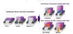
The semiconductor industry is on track to exceed one trillion dollars in annual revenue by the end of the decade, propelled by AI, advanced computing, and edge applications. Yet beneath this growth lies a structural shift. Manufacturing complexity is rising faster than the industry’s ability to manage it. As architectures move deeper into 3D, production disperses globally, and product cycles compress, scale alone is no longer a differentiator. Operational coherence is.

In this environment, competitive advantage increasingly depends on how effectively organizations can learn, decide, and act across organizational boundaries. PDF Solutions’ 2026 priorities reflect a clear recognition of this shift: the company is evolving from a best-in-class analytics provider into a coordination and orchestration platform positioned at the center of the semiconductor ecosystem.

The following analysis reflects PDF Solutions’ stated priorities, positioning, and marketing opportunities based on its most recent Analyst Day presentation.

Manufacturing Analytics as Infrastructure, Not Just Tools

For decades, manufacturing analytics functioned as an overlay. Though powerful, it was disconnected from direct execution. PDF is reframing analytics as infrastructure: a shared data backbone that spans characterization, process development, high-volume manufacturing, test, and assembly. This distinction is critical as data volumes explode and process interactions become increasingly nonlinear.

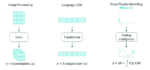
By standardizing how data is ingested, contextualized, and analyzed across domains, PDF’s Exensio platform reduces reliance on custom integrations and tribal knowledge. The result is not simply better visibility, but a common analytical language that enables faster root-cause analysis, more consistent decision-making, and shared accountability across teams and partners. Additionally, it is clear that valuable, trusted, production-ready applications of AI in an industrial context need to be anchored on that type of robust, scalable, and secure data platform. PDF Solutions aims to be the platform enabling the scaling of AI across the semiconductor ecosystem.

Why Analytics Alone Is No Longer Enough

Insight without execution has diminishing value in a distributed manufacturing environment. Analytics can explain what happened and why, but as fabs scale and supply chains fragment, decision latency becomes as costly as yield loss. The next bottleneck is no longer diagnosis but orchestrated execution.

PDF’s strategy reflects this reality. Rather than stopping at insight, the platform embeds analytics directly into manufacturing workflows, ensuring that conclusions translate into aligned action across fabs, test operations, and external partners. This shift moves analytics from advisory to operationally critical.

From Insight to Orchestration

Orchestration is where PDF’s positioning becomes distinctly strategic. Orchestration answers not just “what should happen next,” but also ensures that it actually does. By connecting data, decisions, and actions, PDF enables coordinated responses to yield excursions, prioritizes engineering resources, and synchronizes operations across organizational boundaries.

This evolution is visible in Exensio’s role as an operating layer rather than a standalone analysis environment. It is further reinforced by secureWISE, which extends orchestration beyond the enterprise, enabling standardized, governed data exchange across the broader semiconductor ecosystem. Together, these capabilities position PDF not as another analytics vendor, but as the system that aligns learning and execution at scale.

Orchestration as a Strategic Risk Reducer

As semiconductor manufacturing becomes more globally distributed, coordination failures carry outsized consequences, from delayed ramps to systemic yield losses. Orchestration directly addresses this growing strategic risk. Standardized data exchange and shared workflows enable faster diagnosis, tighter alignment, and more resilient operations across regions and partners.

This elevates platforms like PDF’s from operational tools to strategic assets. The ability to coordinate learning and execution across a fragmented ecosystem becomes as important to resilience as it is to performance.

Secure Data Exchange in a Distributed Ecosystem

Modern semiconductor manufacturing is inherently cross-enterprise. Foundries, OSATs, equipment suppliers, and customers must collaborate without compromising security or IP. PDF’s secureWISE initiative reframes this challenge as a network and standardization problem rather than a series of custom integrations.

By enabling secure, governed data exchange across organizations, secureWISE supports functional consolidation without ownership consolidation. Participants remain independent, but coordinate through shared data models and workflows. As supply chains become more dynamic and geopolitical risk increases, this capability shifts from a differentiator to a requirement.

AI in Manufacturing: Discipline Over Hype

AI is a core pillar of PDF’s platform strategy, but its positioning is deliberately pragmatic. Manufacturing AI operates under constraints that differ sharply from consumer or enterprise applications: low tolerance for error, high accountability, and the need for explainability.

PDF embeds AI within governed analytics environments where models augment engineering judgment rather than replace it. The focus is on productivity, yield improvement, and cycle-time reduction rather than experimentation for its own sake. AI becomes an operational lever, not a speculative bet.

Platform Economics and Financial Leverage

PDF’s technical strategy is reinforced by a clear economic model. The company continues to expand recurring and usage-based revenue streams through subscriptions, cloud deployment, and volume-linked offerings such as secureWISE, Cimetrix, and gainshare. Analytics revenue is growing faster than total revenue, margins are expanding, and backlog growth outpaces the top line, all clear signals of increasing platform maturity.

Importantly, these offerings are becoming embedded deeper into customer operations, positioning PDF’s platform as production infrastructure rather than discretionary IT. This alignment between customer success and revenue growth strengthens financial leverage and durability.

Platform Economics and the Valuation Question: Why This Moment Matters

Despite this evolution, market perception has lagged execution. PDF is still often viewed as a niche analytics specialist rather than a system-level orchestrator. Closing this perception gap represents one of the company’s largest marketing opportunities. The company is working hard trying to change that perception with for example the recent SEMICON WEST keynote given by John Kibarian, PDF Solutions’ CEO emphasizing the need and opportunity for more AI driven collaboration across the semiconductor industry.

The semiconductor industry is approaching an inflection point. Fragmentation, rising complexity, and accelerating demand cycles are colliding with higher capital intensity and tighter talent constraints. Large-scale consolidation is neither practical nor desirable. The more likely outcome is convergence around a small number of coordination platforms that allow diverse ecosystems to function as coherent systems.

PDF Solutions is positioning itself squarely in that role. As a neutral, vendor-agnostic coordination layer, it can benefit from ecosystem fragmentation rather than fight it. When more tools and partners rely on the same platform to share data and coordinate work, the platform naturally becomes more valuable and harder to walk away from. Its future value will be defined less by individual products and more by how deeply it becomes embedded in industry operations.

In an environment where coordination is the new constraint, platforms that enable shared learning and aligned execution may prove to be among the most strategically valuable assets in semiconductor manufacturing.

Learn more at www.pdf.com and here.

Also Read:

Manufacturing Is Strategy: Leadership Lessons from the Semiconductor Front Lines

PDF Solutions’ AI-Driven Collaboration & Smarter Decisions

PDF Solutions Charts a Course for the Future at Its User Conference and Analyst Day


Chiplets Reach an Architectural Turning Point at Chiplet Summit 2026

Chiplets Reach an Architectural Turning Point at Chiplet Summit 2026
by Daniel Nenni on 02-09-2026 at 10:00 am

Chiplet Summit 2026

The semiconductor industry’s transition toward chiplet-based architectures is entering a decisive new phase. What began as a promising alternative to SoC design is now confronting real-world demands around system integration, validation, and long-term scalability. At Chiplet Summit 2026, taking place February 17–19 in Santa Clara, California, Menta will play a prominent role in addressing these challenges, marking its third consecutive year of participation at the event.

Menta, a semiconductor IP and platform company with more than 15 years of experience in programmable and adaptable silicon architectures, has positioned itself as a key architectural voice in the evolving chiplet ecosystem. Originally known for its pioneering work in embedded FPGA (eFPGA) technology, the company has expanded its focus to system-level challenges in advanced and chiplet-based designs. Its continued presence at the Chiplet Summit reflects the industry’s broader shift from conceptual enthusiasm toward industrial validation and deployment.

At Chiplet Summit 2026, Menta returns at what it describes as a pivotal moment. As chiplets move from architectural concepts into production-oriented systems, the dominant challenges are no longer limited to packaging or interfaces. Instead, issues such as architectural coherence, validation under real operating conditions, and the ability to manage heterogeneous systems over long lifecycles are coming to the forefront. Menta will address these topics through a technical presentation, participation in a panel discussion, and on-site engagement at Booth #316.

The company’s technical presentation will focus on architectural decision-making and system-level trade-offs required to design scalable chiplet hubs. These hubs must support long-lived systems while balancing performance, power efficiency, and adaptability. Complementing this, Menta will take part in the panel discussion titled “Selecting the Right Chiplets for Your Edge Application,” which explores how constraints such as power budgets, cost sensitivity, security requirements, communication needs, and limited update cycles shape chiplet choices as intelligence increasingly shifts to the edge.

A central theme of Menta’s participation is the growing need for platforms that go beyond theoretical interoperability. As the chiplet ecosystem matures, the industry faces a critical gap: the lack of environments capable of measuring, comparing, and de-risking modular designs under real-world conditions. Without such platforms, architectural decisions remain difficult to validate before industrial deployment. Menta argues that this gap must be addressed for chiplets to fulfill their promise at scale.

This is where MOSAICS, Menta’s modular chiplet development and validation platform, takes center stage. Initiated at Chiplet Summit 2024, MOSAICS was created to overcome the limitations of monolithic SoC design by providing a universal chassis with standardized interfaces for heterogeneous chiplet systems. By 2026, the platform has reached a significant new phase. A development kit and evaluation platform are scheduled to become available by summer 2026, enabling early adopters to explore and validate modular configurations. The first platform tape-out is planned for the first quarter of 2027, marking a concrete step toward industrial deployment.

MOSAICS is designed to allow real-world measurement and validation of chiplet-based systems, accelerating development cycles and reducing non-recurring engineering costs, particularly for edge and automotive, class applications. By translating architectural vision into an executable platform, Menta aims to provide the structure needed to turn chiplet strategies into reliable, scalable products.

“As chiplets mature, the industry needs fewer promises and more structure,” said Vincent Markus, CEO of Menta, emphasizing the shift from idea-driven discussions to architecture shaping and validation. This perspective underscores Menta’s broader message at Chiplet Summit 2026: the future of chiplets will be defined not only by openness and modularity, but by the ability to prove designs in realistic conditions before they reach production.

Through its technical contributions, platform roadmap, and ongoing engagement with the ecosystem, Menta’s presence at Chiplet Summit 2026 highlights an industry at an architectural turning point, where validation, coherence, and execution are becoming just as critical as innovation itself.

Also Read:

The 71st International Electron Devices Meeting (IEDM 2025)

TSMC’s 2026 AZ Exclusive Experience Day: Bridging Careers and Semiconductor Innovation

DAC – The Chips to Systems Conference 2026


Gate-All-Around (GAA) Technology for Sustainable AI

Gate-All-Around (GAA) Technology for Sustainable AI
by Daniel Nenni on 02-09-2026 at 8:00 am

Gate All Around Technology for Sustainable AI SemiWiki
IEDM 2025 GAA FinFET Paper

The transition from FinFET to Gate-All-Around (GAA) transistor technology represents a pivotal moment in the evolution of logic devices, driven by both physical scaling limits and the rapidly growing computational demands of artificial intelligence. As semiconductor technology approaches the sub-3 nm regime, traditional FinFET architectures face fundamental challenges in electrostatic control, performance scalability, and power efficiency. GAA transistors have emerged not as an optional enhancement, but as an essential foundation for sustaining future logic architectures and enabling sustainable AI computing, absolutely.

FinFETs were introduced to overcome the shortcomings of planar MOSFETs by improving effective channel width and electrostatic integrity through a three-dimensional fin structure. However, aggressive scaling has exposed inherent limitations in this approach. As fin widths shrink, parasitic resistance increases and carrier mobility degrades due to quantum confinement and surface roughness scattering. Additionally, the three-sided gate configuration of FinFETs struggles to adequately suppress short-channel effects at advanced nodes. These issues collectively constrain further scaling, particularly when standard cell heights approach the ~140–160 nm range.

GAA transistors fundamentally address these challenges by fully surrounding the channel with gate material, delivering superior electrostatic control. This all-around gating enables steeper subthreshold slopes, reduced leakage current, and improved short-channel behavior, even at extremely small dimensions. As a result, GAA architectures re-enable cell height scaling to approximately 100 nm and below, restoring performance and power scaling that had plateaued during the later FinFET generations. This capability has driven industry-wide adoption of GAA as the successor to FinFET technology beyond the 3 nm node.

Beyond electrostatics, GAA devices introduce unprecedented design flexibility. Unlike FinFETs, which rely on discrete fin counts to adjust effective width, GAA transistors allow continuous tuning of nanosheet width. This feature enables designers to finely balance speed and power consumption within the same process node. Wider nanosheets support high-performance computing and server applications, while narrower nanosheets reduce power consumption for mobile and AI-centric workloads. This broad coverage across the speed–power spectrum makes GAA particularly well suited for heterogeneous systems and application-specific optimization.

The rise of generative AI and large language models has further amplified the importance of GAA technology. AI workloads demand exponential growth in compute capability, pushing systems toward petascale and exascale performance levels. At the same time, global data center power consumption is projected to increase dramatically, raising concerns about energy sustainability. GAA transistors directly address this tension by enabling higher performance per watt and supporting increased SRAM density. Higher on-chip memory density reduces off-chip data movement, improving data locality and lowering energy costs associated with high-speed interconnects.

Crucially, GAA also serves as a structural platform for future transistor innovations. Architectures such as Forksheet FETs and three-dimensional stacked FETs (3DSFETs) build directly upon the GAA concept, preserving its electrostatic advantages while enabling further area scaling. When combined with backside power delivery networks, these advanced structures offer improved routing efficiency, reduced voltage drop, and enhanced overall performance. Together, these innovations position GAA as the cornerstone of “beyond-GAA” logic technologies.

Bottom line: The transition to Gate-All-Around technology marks a foundational shift in semiconductor design. GAA is not merely a replacement for FinFETs, but a scalable, flexible, and energy-efficient platform capable of supporting future logic architectures and sustainable AI growth. As device scaling continues to confront physical and power-related constraints, the successful implementation of GAA will determine the industry’s ability to meet the performance, efficiency, and societal demands of next-generation computing.

Also Read:

The 71st International Electron Devices Meeting (IEDM 2025)

DAC – The Chips to Systems Conference 2026

Verification Futures with Bronco AI Agents for DV Debug


VSORA Board Chair Sandra Rivera on Solutions for AI Inference and LLM Processing

VSORA Board Chair Sandra Rivera on Solutions for AI Inference and LLM Processing
by Lauro Rizzatti on 02-09-2026 at 6:00 am

Sandra Rivera VISORA

Sandra Rivera, a Silicon Valley veteran who is the former CEO of Altera, an Intel FPGA spinout, and long-time Intel executive, recently became Chair of the Board of Directors of Paris-based VSORA. VSORA, a technology leader redefining AI inference for next-generation data centers, cloud infrastructure and edge, is focused on addressing high-performance, low-latency inference use cases, a market that is expected to grow to $250B by 2029.

I recently had a chance to talk with Rivera to find out more about what she sees as VSORA’s strengths and opportunities.

Rizzatti: What specific technical bottlenecks in the current AI hardware landscape convinced you that VSORA’s unique architecture provides a solution?

Rivera: One of the things we know now, in terms of the AI industry and the juncture that we’re at, is that the bottleneck for more scalable deployments is not in raw compute—it is absolutely about data movement. And if you look at the current architectures being deployed, they’ve been focused more on heavy training workloads, which GPUs are more suited.

If you look at the problem we’re trying to solve around AI inference—particularly for large models and real-time workloads—we know that performance is not constrained by compute, but by memory bandwidth, latency, and determinism,.

When we look at the problems customers are expressing to us, they want a solution that addresses high throughput, low latency, and a more deterministic set of requirements that they need to deploy in their environments. And VSORA’s architecture directly attacks this problem in terms of how data flows through the system. It minimizes off-chip memory access, maximizes effective bandwidth, and delivers much more predictable latency.

What we’re hearing from customers is that current solutions are increasingly underutilized for inference—perhaps even over-engineered for inference. They’re expensive to scale and power-hungry, whereas the VSORA architecture and product are compelling because they are built specifically to address this bottleneck: high-bandwidth, low-latency, scalable inference.

And these solutions are also quite cost-effective compared to the power-hungry GPUs that were designed to address a different part of the workflow, mainly training.

Rizzatti: Nvidia acquired Groq. Its architecture differs from that of VSORA, but at a 30,000-foot view, the problem it is addressing is similar. Do you view this acquisition as an implicit acknowledgement by Nvidia that the GPGPU is not doing the proper job for LLM processing?

Rivera: The investment by Nvidia in Groq certainly reinforces the position we’ve taken regarding the problem we’re focused on solving. It validates the thesis for the VSORA business, which is that customers are increasingly looking for solutions to address the AI inference problem.

This is about power efficiency, cost per token, and certainly much lower latency and more determinism than you’re able to get from more general purpose computing architectures.

So yes, it’s quite helpful, because the market leader is acknowledging that it is not a one-size-fits-all architecture for addressing all the different elements of an overall AI workflow. Indeed, you need heterogeneous architectures that address different areas of that AI continuum.

For us, it’s a strong validation that the thesis we had—focusing on what is probably the biggest pain point and the largest market opportunity in the coming years—is correct: low-latency, high-performance inference that is cost-effective and power-efficient. And with our innovative architecture, we address those problems head-on.

Rizzatti: In a previous chapter, the VSORA team founded, built, and successfully exited a company called DibCom, an innovator in radio decoding that developed an advanced digital signal processor. In many ways, it laid the groundwork for VSORA. Are you confident this same team can achieve a similar level of success in AI.

Rivera: One of the biggest appeals for me in joining the team—and for prospective customers considering VSORA solutions—is the fact that this is a team that has been working together and delivering products for many years.

They have had 14 successful tape-outs in their history. They have now taped out a very complex logic device on leading process technology, including advanced packaging technology and high-bandwidth memory embedded into the overall platform.

It is not an easy thing for organizations, and certainly for silicon development teams, to come together and deliver complex products. The fact that this team, with this particular leader—the CEO—has done that 14 times before, and now has done it once again in an fast-moving field like AI, really demonstrates the cohesiveness of the team and the deep experience and expertise they have in developing complex silicon products.

I think it is one of the biggest differentiators of VSORA compared with many of the new startups that don’t necessarily have a history of working together or a demonstrated track record of success.

I consider this one of the major positives that prospective customers can feel confident about when choosing VSORA solutions for their AI infrastructure.

Rizzatti: Do you agree or disagree with the “one size doesn’t fit all” narrative that a few major players in AI processing promote? How does VSORA fit into this narrative?

Rivera: As I said earlier, the industry is very much moving toward heterogeneous architectures that address the entire AI workflow.

Even if you look at the role of the CPU as the head node and orchestrator, it handles preprocessing and data cleaning before training. GPUs and highly parallel architectures used effectively for training-heavy workloads with massive frontier models.

Then you move into architectures designed for specific parts of the workflow and different applications. Some focus on media processing, some on networking throughput and others on storage acceleration.

In our case, we are focused on efficient data movement between the processing engine and external memory. We have a unique architecture that addresses the memory wall problem where compute units stall waiting for data, resulting in wasted performance and excessive power draw.  Our award-winning, patented architecture enables a very power-efficient, low-latency, and low-cost solution for the AI inference problem.

The need for heterogeneous architectures to address the varying AI workload requirements is not just my belief – you’re seeing a number of strategic partnerships, collaborations, and acquisitions in the industry to support this approach..

Lauro: 2025 was defined by the race to scale. As we look forward to 2026 and beyond, what would you predict to be the main trends?

Rivera: I think the next phase will be defined much more around efficiency, specialization, and economics—going back to having the right architecture for the right part of the workload.

All the data and analyst research show that inference is going to dominate in terms of what enterprises are looking to address for large-scale deployments.

Problems around latency, power efficiency, and deployment costs will matter much more than headline peak benchmark numbers, which is how much of the industry has evaluated solutions to date.

I think we will also see tighter coupling between software and hardware, and architectures specifically designed for inference characteristics will shine compared to solutions repurposed from training accelerators.

In that market landscape, and in meeting customer requirements, VSORA is very well positioned—not because we seek to be different, but because we are aligned with customer pain points and where the market is heading.

We believe we will be a major player in enabling AI to scale sustainably, not just because of the technical solution, but also because of the commercial attractiveness of the offer.

Contact VSORA

Also Read:

CEO Interview with Naama BAK of Understand Tech

CEO Interview with Dr. Heinz Kaiser of Schott

CEO Interview with Moshe Tanach of NeuReality


TSMC & GCU Semiconductor Training Program: Preparing Tomorrow’s Workforce

TSMC & GCU Semiconductor Training Program: Preparing Tomorrow’s Workforce
by Daniel Nenni on 02-08-2026 at 2:00 pm

TSMC GCU Semiconductor Training Program

The expansion of semiconductor manufacturing in the United States, particularly with TSMC’s multi-fab campus in Phoenix, Arizona, has created a significant need for skilled technical workers. To meet this demand, TSMC has partnered with educational institutions, including Grand Canyon University (GCU), to launch innovative training pathways aimed at preparing individuals for careers in semiconductor fabrication and operations. This partnership is part of a broader ecosystem effort involving government, workforce boards, community colleges, and universities working together to develop a sustainable talent pipeline for the semiconductor industry.

Why the Program Exists

Semiconductor manufacturing is one of the most technically demanding and high-technology sectors in the global economy. Operating advanced fabrication facilities, or “fabs”, requires talent with specialized skills in automated systems, precision processes, cleanroom operations, and semiconductor science. When TSMC announced its Arizona investment, one of the key challenges highlighted was the shortage of locally available semiconductor workforce talent with requisite technical skills. In response, the company and regional partners have collaborated on training and apprenticeship programs to build that talent ecosystem locally.

Program Structure and Partnerships

The TSMC-GCU semiconductor training program, formally known as the Manufacturing Specialist Intensive Pathway, is an industry-aligned educational pathway created to prepare participants for technical roles within semiconductor manufacturing. This initiative is part of a broader suite of workforce development efforts that also include registered apprenticeship programs, technician training with community colleges and Northern Arizona University, and other industry partnerships.

At its core, the program with Grand Canyon University focuses on equipping individuals with practical skills that map directly to Manufacturing Specialist roles at TSMC’s Phoenix fabs. The curriculum encompasses semiconductor fundamentals, wafer fabrication processes, standard operational procedures, and factory-floor workflows, all of which are foundational knowledge areas for anyone seeking to enter semiconductor manufacturing.

Program Details

Duration & Format: The program typically runs over a 15-week period, blending classroom instruction with industry-relevant learning experiences designed to mirror real semiconductor manufacturing environments.

Credentialing: Participants earn a certificate of completion from GCU, along with 16 college credit hours, and industry-recognized professional credentials from the Institute of Electrical and Electronics Engineers (IEEE), which helps validate competencies to employers.

Target Audience: The training is geared toward a wide range of learners — from high school graduates and career changers to individuals already in the workforce seeking new tech-focused opportunities.

Pathway to Employment: Successful participants gain not only educational credentials but also a competitive advantage when applying for semiconductor technician, manufacturing specialist, or related technical roles at TSMC or other semiconductor firms in Arizona.

Broader Workforce Strategy

While the GCU partnership is a key piece of the talent development puzzle, it sits within a larger regional workforce strategy. TSMC’s Registered Technician Apprenticeship program, supported by the State of Arizona, the City of Phoenix, and institutions like Estrella Mountain Community College, Northern Arizona University, and other partners, offers multi-year apprenticeship pathways in equipment, process, and facilities technician roles that combine classroom instruction with paid on-the-job training.

These programs are designed to address both entry-level and advanced technical needs. Apprentices typically work hands-on in real semiconductor environments while earning credit and experience, which can lead to stackable credentials and even associate or bachelor’s degrees when combined with college coursework.

Impact and Future Prospects

The TSMC-GCU semiconductor training program underscores the importance of public-private educational collaboration in scaling a skilled workforce fast enough to match the pace of industrial growth. By equipping participants with relevant technical knowledge and credentials recognized by both academia and industry, the program not only fills immediate labor gaps but also fosters long-term career opportunities in a high-tech sector that is becoming increasingly critical for U.S. competitiveness.

Bottom line: This initiative helps bridge the transition from education to employment in a field where the demand for skilled workers is projected to grow as semiconductor manufacturing continues to expand across the United States.

GCU and TSMC’s MSI Pathway Webinar

Also Read:

The Chronicle of TSMC CoWoS

TSMC’s CoWoS® Sustainability Drive: Turning Waste into Wealth

TSMC’s 6th ESG AWARD Receives over 5,800 Proposals, Igniting Sustainability Passion


CEO Interview with Dr. Raj Gautam Dutta of Silicon Assurance

CEO Interview with Dr. Raj Gautam Dutta of Silicon Assurance
by Daniel Nenni on 02-08-2026 at 12:00 pm

Dr. Raj Gautam Dutta


Dr. Raj Gautam Dutta is the Co-Founder and Chief Executive Officer of Silicon Assurance, where he defines the company’s strategic direction and leads its technology and product vision. He is responsible for driving the development of differentiated hardware security solutions, executing growth and partnership strategies, and positioning the company within the global semiconductor and security ecosystem. With over eight years of experience in hardware security innovation, Dr. Dutta has a proven record of translating advanced research into deployable, market-ready technologies. His background in technology transfer and strategic technology analysis enables Silicon Assurance to deliver solutions that combine deep technical rigor with commercial and mission-critical relevance.

Tell us about your company

Silicon Assurance is a Security EDA company dedicated to strengthening semiconductor supply chain trust by enabling organizations to establish verifiable confidence in the security of the silicon they design, integrate, procure, and deploy. Our flagship platform, Analyz-N™, is a gate-level security assurance platform that automates the identification of security-relevant assets, analyzes post-synthesis security risk, and generates audit-ready assurance reports to prove customers’ silicon is verifiably secure, not merely assumed secure.

What problems are you solving?

Modern microelectronics underpin mission-critical cyber and national security systems, yet hardware security assurance has not kept pace with the sophistication of emerging threats. The complexity of AI accelerators, the rise of multi-chiplet architectures, and pervasive third-party IP reuse have significantly expanded the hardware attack surface and weakened traditional trust boundaries. Current practices rely heavily on RTL-focused point tools and static checklists, which fail to capture evolving hardware threats and the security implications of EDA design and verification flows that were not built with adversarial behavior in mind. As a result, vulnerabilities—such as leakage paths, privilege escalation, hardware Trojans, or countermeasures that fail to propagate through synthesis—can remain undetected until post-deployment.

Silicon Assurance is developing Analyz-NTM, an end-to-end automated gate-level security assurance EDA platform designed to prove the security of microelectronics. Our flagship platform’s capabilities include automatically identifying security-relevant assets, correlating them with common security weaknesses, analyzing post-synthesis security risk, identifying attack stimuli, locating the source of weakness, and generating security testbenches. This allows customers to detect security degradation before silicon is built and to prove, rather than assume, that their silicon is secure.

What application areas are your strongest?

We are strongest in high-assurance and mission-critical applications, including defense, aerospace, critical infrastructure, and automotive. Our platform is particularly valuable for designs where a single security failure can lead to system compromise, safety risks, or national security impacts.

What keeps your customers up at night?

Customers worry about unknown security vulnerabilities in their designs, which can lead to system recalls and the remanufacturing of chips. They are concerned about auditability, compliance, and proving their chips are secure for their customers.

What does the competitive landscape look like and how do you differentiate?

Existing solutions fall into three categories:
● Traditional EDA tools: Focused on functional correctness and performance, not adversarial security behavior.
● Manual security reviews: Expert-driven but slow, subjective, limited in coverage, and unscalable.
● Point security tools: Designed for RTL analysis and narrow in scope, i.e., focus on a subset of collaterals generated by Analyz-N .

Silicon Assurance differentiates by being security-first, implementation-aware, scalable, exhaustive, and autonomous, positioning it to define hardware security verification as a core requirement for silicon designs rather than an ad-hoc review step.

What new features or technology are you working on?

We are combining GenAI-driven formal analysis, rule-based analysis, fuzzing-style exploration, and AI-driven reasoning into the Analyz-N platform to make it accessible to entry-level security verification engineers. Furthermore, such technologies will enable Analyz-N to detect various threat categories. The platform’s results are repeatable, verifiable, accurate, and scalable to modern hardware designs, enabling forward integration into commercial design flows.

How do customers normally engage with your company?

Customers typically engage through pilot evaluations on real IPs or SoCs, where we demonstrate concrete, design-specific findings. From there, we move into enterprise deployments aligned with existing verification flows and simulators. Our engagements are highly collaborative. We work closely with security, verification, and design teams to integrate Analyz-N into their design and verification lifecycle.

LEARN MORE

Also Read:

CEO Interview with Naama BAK of Understand Tech

CEO Interview with Dr. Heinz Kaiser of Schott

CEO Interview with Moshe Tanach of NeuReality


Podcast EP330: An Overview of DVCon U.S. 2026 with Xiaolin Chen

Podcast EP330: An Overview of DVCon U.S. 2026 with Xiaolin Chen
by Daniel Nenni on 02-06-2026 at 10:00 am

Daniel is joined by Xiaolin Chen, Senior Director of Technical Product Management for Formal Solutions at Synopsys. She has over 20 years of experience applying formal technology in verification and partnering with customers to identify opportunities where formal methods are best suited to solve complex verification challenges. She is currently serving as the General Chair for DVCon U.S. 2026 and has been on the steering committee and has been serving as a member of technical program committees since 2019. She has also authored more than 20 conference papers and holds a patent.

Dan explores the upcoming DVCon event with Xiaolin. The conference will be held at the Hyatt Regency Santa Clara from March 2-5, 2026. Xiaolin explains that the Hyatt Regency is a new venue for the event. Its larger size will allow more events and larger sessions. The conference has grown quite a bit and this year there are four Platinum sponsors. Xiaolin explains that this allows a larger number of sponsored events creating a very full agenda.

Dan reviews the keynotes, tutorials, workshops, paper sessions, interactive poster sessions, and panels that are planned. There is also a hackathon. Xiaolin explains there are several high-profile keynote speakers. A main focus for many conference events is the application of AI. Dan and Xiaolin explore the implications of AI for design verification in some detail.

You can register for DVCon USA here.


The Risk of Not Optimizing Clock Power

The Risk of Not Optimizing Clock Power
by Mike Gianfagna on 02-06-2026 at 6:00 am

The Risk of Not Optimizing Clock Power

Clock power is rarely the issue teams expect to limit advanced-node designs. Yet in many chips today, over-driven clock networks quietly consume disproportionate power, reduce thermal headroom, and can constrain achievable frequency. And all while passing traditional sign-off checks and often remaining locked in through tapeout.

Because clocks toggle continuously and span the entire chip, inefficiencies in the clock network compound relentlessly. Once locked into silicon, these costs are paid every cycle, in every product, for the life of the design. Let’s take a closer look at the risk of not optimizing clock power.

Power as a Silent Constraint

Power is a universal constraint for advanced chip designs, increasingly determining whether performance targets, thermal limits, and product differentiation can actually be achieved. While designers spend significant effort optimizing functional logic, the clock network often escapes the same level of scrutiny because it is assumed to be good enough once timing closes, even though power behavior is no longer explicitly examined in a detailed, clock-network-specific way.

Why Clock Power Is Getting Worse

The massive processing required by AI workloads has turbo-charged the problem. There are many dials to turn to optimize power. It turns out the energy consumed by the clock network in most advanced designs is a substantial contributor to the power problem – often without being explicitly identified as such during sign-off, even as logic efficiency improves and overall power budgets tighten. Clock power can quietly erode available budget even when all timing requirements appear to be met.

Clock Networks: A Disproportionate Power Consumer

You can do your own research on the issue. I found some very useful data at numberanalytics.com and embedded.com. A few key statistics are worth repeating:

  • In modern chips, clock networks can account for over 50% of the total dynamic power consumption.

Several factors contribute to the power consumption of clock networks:

  • Capacitance: The capacitance of the clock network affects how much power is consumed during signal transitions.
  • Switching Activity: The frequency at which the clock toggles directly impacts power usage. Higher switching rates lead to increased power consumption.
  • Wire Length: Longer wires increase resistance, which can lead to higher power dissipation.

Capacitance, switching activity (or clock speed), and wire length are all familiar problems for advanced chip design. They all drive power consumption in the wrong direction.

It’s also important to note that unlike logic nets, which may toggle infrequently, the clock net has a 100 percent activity factor. Every inefficiency in gate sizing, topology, or loading assumption is therefore paid continuously. Small amounts of excess drive strength can translate into significant power loss when multiplied across deep clock networks and sustained over billions of cycles. This makes clock power uniquely unforgiving: inefficiencies do not average out over time.

Where Traditional Clock Power Analysis Falls Short

Let’s look at some of the basic steps of how the clock tree is implemented:

  1. RTL design of clock network, considering items such as net connectivity, number of nodes, required drive strength and estimate wiring load.
  2. Synthesize the clock tree.
  3. Perform post layout extraction and timing analysis to verify the clock network meets timing specifications. At this stage, the clock network is typically judged complete based on timing closure alone. Once this judgment is made, opportunities to revisit clock power late in the flow are often avoided due to perceived risk.

This is clearly a simplified view of the steps involved, but what happens in step 3 presents a significant opportunity. Tools like static timing analysis can verify overall performance of the clock network to ensure timing is met. But at what cost?

The opportunity here lies in the clock gates that are inserted during synthesis. The choices made by the synthesis tool are influenced by the drive requirements of the elements in each clock tree and an estimate of the loading effects of the wiring. The amount of wiring has become quite large for advanced designs, so small errors in estimates can become big discrepancies in the final layout.

In any clock network, there will be drivers that are too large for the required load, resulting in wasted power. There will also be undersized drivers that will struggle to keep up, also wasting power, though over-sizing is far more common in practice.

A useful analogy here is internal combustion engines in automobiles. If the engine is too small for the car’s weight, it will struggle and waste gasoline. If it’s too powerful for the car’s weight, gas will also be wasted. There is an optimal engine size for a given car configuration from a fuel efficiency point of view. The same is true for clock network drivers.

This combination of scale, electrical complexity, and late-stage risk has made clock power one of the hardest problems to address in practice. The post-layout netlist of the clock network contains all the actual wiring load and clock drivers chosen by the synthesis tool. Some of those drivers will be too small for the required load and some will be too large, based on the difference between the estimate and actual wire loads.

The most reliable way to find these issues is to perform a SPICE-level analysis on the clock network. Historically, this level of electrically accurate analysis has been impractical at full clock-network scale. Until now, this level of analysis was impractical for real designs.

Turning Clock Power Risk into an Addressable Problem

ClockEdge has developed technology that makes electrically accurate clock power analysis practical at full scale – an area that has traditionally been out of reach. Instead of relying on inferred models or averaged assumptions, this approach evaluates clock power behavior directly across complete clock networks under realistic post-layout conditions.

Crucially, this visibility can be applied early in the clock design process, beginning at clock tree synthesis (CTS). By identifying over-driven paths and unnecessary margin at CTS, teams can make informed sizing and topology decisions before inefficiencies are propagated and locked in. This early intervention reduces downstream power waste and minimizes the need for disruptive late-stage changes.

As the design matures, the same electrically grounded analysis continues to provide value, allowing teams to validate clock power assumptions and refine optimization decisions with confidence. By anchoring analysis in actual electrical behavior, clock power optimization becomes a controlled, data-driven exercise rather than a risky late-stage guess – while preserving timing integrity throughout the flow.

Clock power is no longer a secondary concern- it is a growing source of hidden risk in advanced-node designs. When conservative assumptions are embedded early in CTS and left unexamined, unnecessary power consumption can become locked in, quietly constraining performance, thermal headroom, and predictability. The risk of not optimizing clock power is that its impact often goes unnoticed until it’s too late to change.

To Learn More

If clock power is expected to challenge your next design, ClockEdge provides a practical solution to evaluate and optimize clock power using its vPower solution. To see how this technology applies to your clock network before inefficiencies are locked in, request a demo with the ClockEdge team. This is how you can avoid the risk of not optimizing clock power.

Also Read:

Taming Advanced Node Clock Network Challenges: Jitter

Taming Advanced Node Clock Network Challenges: Duty Cycle

How vHelm Delivers an Optimized Clock Network


Quadric’s Recent Momentum & Funding Success

Quadric’s Recent Momentum & Funding Success
by Daniel Nenni on 02-05-2026 at 10:00 am

Quadric Chimera GPNPU

Quadric®, Inc., headquartered in Burlingame, California, is accelerating its position as a leading provider of programmable AI inference processor intellectual property (IP) and development tools for on-device AI workloads. The company announced an oversubscribed $30 million Series C funding round, bringing total capital raised to $72 million. This round was led by the ACCELERATE Fund (managed by BEENEXT Capital Management), with participation from returning investors: Uncork Capital and Pear VC, as well as new investors: Volta, Gentree, Wanxiang America, Pivotal, and Silicon Catalyst Ventures.

According to Quadric and reporting by industry outlets, this Series C comes as product revenues more than tripled in 2025 compared to 2024, reflecting strong adoption of the company’s technology across multiple application areas including edge large language models (LLMs), automotive AI processing, and enterprise vision workloads. Executives point to “accelerating design-win momentum” as proof of increasing market traction for Quadric Chimera™ general-purpose neural processor architecture.

Quadric positions its Chimera™ IP as a fully programmable alternative to fixed-function NPUs that typically dominate the edge AI landscape. Chimera supports both traditional DSP and AI inference tasks on a unified architecture, enabling semiconductor designers to build chips capable of running vision models and on-device LLMs (including models up to ~30B parameters). The architecture is scalable from 1 trillion operations per second (TOPS) up to 864 TOPS, with automotive-grade, safety-enhanced options for ASIL compliance.

Management has emphasized that this software-centric, programmable approach helps shield customers from the risk of obsolescence as model architectures evolve— an advantage over rigid accelerators in a fast-changing landscape.

Strategic License Wins & Ecosystem Expansion

In conjunction with the funding announcement, Quadric also disclosed new licensing wins that underscore the diversity of its target markets. One new licensee is a leading Asia-based edge-server LLM silicon provider, reflecting demand for on-device language model inference at scale.

A second major engagement comes from TIER IV, Inc. of Japan, a leader in autonomous driving software. TIER IV has licensed the Chimera AI processor software development kit (SDK) to evaluate and optimize future iterations of Autoware®, the open-source autonomous vehicle software stack the company pioneers.

The TIER IV engagement illustrates Quadric’s push into automotive and autonomous system markets, where efficient, programmable AI compute is increasingly a differentiator. As AI workloads proliferate in next-generation vehicles—handling perception, planning, and control—Quadric’s SDK provides a pathway for developers to optimize inference for the specific needs of autonomous platforms.

Leadership & Organizational Developments

Quadric has been strengthening its leadership and engineering bench. In December 2025, the company announced the appointment of Ravi Chakaravarthy as Vice President of Software Engineering, a role focused on driving the development of the embedded AI software stack that underpins the Chimera IP and toolchain.

Around the same time, Quadric also added Joachim Kunkel as an independent member of its Board of Directors. Kunkel brings deep industry experience, particularly from his 18-plus years leading Synopsys’ semiconductor IP division. His participation signals Quadric’s intent to scale strategically and benefit from seasoned guidance as it expands its footprint in the AI processor IP ecosystem.

Market Context & Competitive Stance

Quadric’s progress comes against a backdrop of consolidation in the neural processing unit (NPU) IP market. According to industry reporting, the number of startups offering NPU IP has declined as competition intensifies and differentiation becomes more difficult. Quadric’s blend of programmable hardware and comprehensive software tooling is cited by some observers as a key competitive advantage that helps it stand out from both fixed-function accelerator vendors and other IP licensors.

Bottom Line: With this recent funding and expanding customer engagements, Quadric appears positioned to continue its strategy of licensing the Chimera IP and SDK to chipset designers tackling the diverse demands of edge AI, in areas ranging from smart devices and industrial systems to advanced driver assistance and autonomous vehicles.

Quadric also has a new website which, as a website connoisseur, I find quite clever. Click here and check it out.

Also Read:

Quadric: Revolutionizing Edge AI

Legacy IP Providers Struggle to Solve the NPU Dilemna

Recent AI Advances Underline Need to Futureproof Automotive AI


Beyond Transformers. Physics-Centric Machine Learning for Analog

Beyond Transformers. Physics-Centric Machine Learning for Analog
by Bernard Murphy on 02-05-2026 at 6:00 am

Physics based learning

Physical AI is an emerging hot trend, popularly associated with robotics though it has much wider scope than compute systems interacting with the physical world. For any domain in which analysis rests on differential equations (foundational in physics), the transformer-based systems behind LLMs are not the best fit for machine learning. Analog design analysis is a good example. SPICE simulators determine circuit behavior by solving a set of differential equations governed by basic current and voltage laws applied to circuit components together with boundary conditions. Effective learning here requires different approaches.

Machine learning methods in analog

The obvious starting point is to run a bunch of SPICE sims based on some kind of statistical sampling (across parameter and boundary condition variances say) as input to ML training. Monte Carlo analysis is the logical endpoint of this approach. For learning purposes, such methods are effective but significantly time and resource consuming. Carefully reducing samples will reduce runtimes, but what will you miss in-between those samples?

A different approach effectively builds the Newton (-Raphson) iteration method behind SPICE into the training process, enabling automated refinement in gradient-based optimization. (Concerns about correlation with signoff SPICE can be addressed through cross-checks when needed.)

Newton ‘s method is the gold standard in circuit solving but is iterative which could dramatically slow learning without acceleration. Parallelism provided the big breakthrough that launched LLMs to fame. Could the same idea work here? The inherent non-linear nature of analog circuit equations has proven to be a major challenge in effectively using parallelism for real circuits. However a recent paper has introduced an algorithm allowing for machine learning with embedded circuit sim to more fully exploit parallelism using hardware platforms such as GPUs.

Beyond sampling to deep physics modeling

At first glance, simply embedding circuit solving inside a machine learning (ML) algorithm seems not so different from running sims externally then learning from those results. Such a method would still be statistical sampling, packaged in a different way. Mach42  have a different approach in their Discovery Platform which they claim leads to higher accuracy, stability and predictive power in results. I see good reasons to believe their claim.

Brett Larder (co-founder and CTO at Mach42) gave me two hints. First, they aim for continuous time modeling during ML training, whereas most digital methods discretize time. They have observed that conventional methods predict results which are noisy, irregular, even inaccurate, whereas in their algorithm each training point can contain measurements at a different set of time values, rather than requiring that each index on an input/output always correspond to the same time. Training data distributed across timepoints rather than bunched into discretized time steps; I can see how that could lead to more accurate learning.

Second, they aim to learn parameters of the differential equations describing the circuit, rather than learning coarse statistical sampling of input to output results. This is very interesting. Rather than learning to drive a model for statistical interpolation, instead it learns refined differential equations. For me this is intuitively more likely to be robust to changes under different physical conditions and truly feels like deep physics modeling.

The cherry on the cake is that this algorithm can be parallelized to run on a GPU, making training very time-efficient, from SerDes at 2 hours to a complex automotive PMIC at 20 hours, all delivering accuracy at 90% or better. The models produced by this training can run inside SPICE or Verilog-A sims, orders of magnitude faster than classical AMS simulations.

Payoff

Active power management in devices from smartphones to servers depends on LDOs providing regulated power to serve multiple voltage levels. A challenge in designing these circuits is that the transfer function from input to output can shift as current draw and other operating conditions change. Since the goal of an LDO is to provide a stable output, compensating for such shifts is a major concern in LDO design.

The standard approach to characterizing an LDO is to run a bunch of sweeps over circuit parameters to determine how well compensation will manage across a range of load and operating conditions. These simulations consume significant time and resources and can miss potential issues in-between sweep steps. In contrast, the learned dynamic model created by the Discovery Platform provides much more accurate estimation across the range, so that anomalies are much more likely to be detected. Moreover, changes in behavior as parameters are varied can be viewed in real-time thanks to these fast dynamic models.

Very nice – moving beyond transformer-based learning to real physics-based learning. You can read more about this new modelling approach in Mach42’s latest blog HERE.

Also Read:

2026 Outlook with Paul Neil of Mach42

Video EP12: How Mach42 is Changing Analog Verification with Antun Domic

Video EP10: An Overview of Mach42’s AI Platform with Brett Larder