R&D for any fundamentally new technology takes time, especially for hardware; over 10 years passed from the first transistor to the first (very small) integrated circuit. The engineering behind quantum computers is arguably even more challenging than for electronic circuits, at least from today’s perspective. We shouldn’t be surprised that even now there are more challenges to overcome. As usual, for a quick read I will look at just a couple, a gate essential to demonstrating quantum advantage over classical computing, and quantum error correction (QEC) / fault-tolerant architectures.
T-gates
Introductions to quantum programming start with a simple set of gates called the Clifford group: H, S, and C-NOT gates. This group is important in many aspects of quantum programming and has the added advantage that algorithms based on the group can be simulated classically as efficiently as in quantum implementations. However the group is not complete for supporting general calculations, especially for algorithms that would be exponentially complex to compute on a classical system.
T-gates are a popular option to extend the set. Skimming over the details, gates in the Clifford group can modify a qubit through a very limited set of possibilities. A T-gate extends the range and can be thought of as the square root of an S gate (equivalent to S if applied twice). When combined in a sequence with Clifford gates this enables any arbitrary operation on a qubit to some desired accuracy. (Might seem surprising but the math goes all the way back to Euler.)
That’s the theory. How can a T-gate be implemented on a real quantum computer (QC)? Looking back at a couple of my earlier blogs on QC implementation (this and this), you’ll remember that gates are implemented by pulsing qubits with microwave, laser or other EM options. Naturally these mechanisms have imperfections, including finite frequency spread in pulses and imperfect focusing optics for lasers.
Add ambient noise on top of these imperfections and you can see that any intended gate operation will be performed with less than perfect fidelity. Clifford group states are in some sense maximally separated so perhaps a little less prone to errors, but a T-gate operation, as a square root of a Clifford gate, will typically be more sensitive.
The QC experts have an answer to this need. In one example, they pre-build one or more sets of purified T-gates, distilled from multiple noisy T-gates. In this approach, when considering your target algorithm, the number of T-gates you will need must be pre-determined along with the level of accuracy you must meet.
I expect the mechanism to purify T-gates will be captured in a library though given constraints on available qubit and coherence times for production systems today, any bloat will further limit allowable size and duration of your algorithm. Adding this new gate also adds complexity to verifying an algorithm on a classical computer, since complexity on a classical system grows exponentially with the number of T-gates. Recent research has shown it is possible to simulate relatively shallow circuits with T-gates so there is still hope for debugging noisy quantum circuits.
QEC and fault-tolerant computing
I touched on QEC in my blog on physical implementation of quantum computers. I’ll expand a bit more here. The basic concept in QEC is the same as in classical error correction – “copy” onto redundant qubits, run an operation, detect single qubit errors through majority voting and correct any errors (also work hard to make the probability of 2 or more errors very small). An operation starts with a qubit, adds redundancy, performs the operation, detects and corrects errors, from that reconstructing a corrected post-operation qubit.
There are complications.
Simply copying real qubits breaks coherence, instead they are entangled with the redundant qubits. After an operation, the method detects incorrect entangled states and uses that result to correct errors. However, qubit error possibilities aren’t just bit-flips; they can also be phase flips (e.g. |0>+|1> flips to |0>-|1>), requiring more circuitry to detect and correct. QEC around gates outside the Clifford group (like a T-gate) is more complicated to protect. Of course, error detection and correction circuitry will contribute further errors.
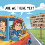
If this sounds difficult, you are not wrong. This is a race between error creation and error detection and correction. Some views held that ~1000 physical qubits would be required per logical qubit, clearly not scalable. Very active research is going into this area, in higher reliability qubits and in fault-tolerant computing, computing with accuracy using faulty systems.
I can’t find data on superconducting versus ion trap qubit reliabilities. Before considering external noise, I feel that ion trap reliabilities should be intrinsically high simply thanks to the physics of a single ion, whereas manufactured superconducting qubit will have inevitable tolerance errors.
IBM recently published breakthrough results, to reduce noise in memory (a set of qubits) though this does not touch on gate operations. Here is a nicely readable version, including some background on evolution of error correcting codes from Hamming to surface codes and now their latest “gross code”. For gate operations IBM points to next steps in the readable link immediately above. I couldn’t find reported results. In my (possibly faulty 😀) reading this suggests greatly reduced overhead for error correction, partly through choice of error-correcting codes and partly through pre-distillation of more error-prone operations such as T-gates (see above).
More background
There is a great video tutorial series from Artur Ekert (professor of quantum physics at Oxford) that I mentioned in an earlier blog. This is a deep dive into quantum information science, not for the timid or anyone looking for a quick summary. But I found it illuminated many points for me, especially in viewing any quantum computation as essentially a very elaborate quantum interference experiment. If you are familiar with regular wave interference (drop 2 stones in a pond and watch how the ripples interact) and/or the double-slit experiment this will make complete sense.
Also Read:
Simulating Quantum Computers. Innovation in Verification