At the TERAFAB launch event in Austin on March 21, Elon Musk made a prediction that would have sounded like science fiction a decade ago—and may still: roughly 80 percent of AI compute will eventually move off-planet.
The argument is straightforward once you accept his premises. Earth-based data centers face three hard constraints—land, cooling, and grid capacity—and all three are getting worse as AI infrastructure demand accelerates. Land requires zoning, permitting, and proximity to fiber and power. Cooling consumes enormous quantities of water or electricity, or both. And grid capacity, particularly clean grid capacity, is increasingly contested.
Space, Musk argues, dissolves all three simultaneously. Satellites don’t need real estate. The vacuum of space is an ideal radiative heat sink—no water, no chillers, no mechanical systems at all. And solar irradiance above the atmosphere runs roughly five times the average output of a ground-based installation—not because the sun shines harder in space, but because a space-based array sees the sun continuously, with no night cycle, no weather, and no atmospheric losses. It is, Musk suggested, basically a free data center—if you can get there.
The obvious objection is launch cost. Getting hardware into orbit remains expensive by any terrestrial comparison. Musk’s counter is that Starship changes the math, and TERAFAB—announced the same evening, in a defunct Austin power plant, with light beams shooting into the sky and the Governor of Texas in the audience—changes it further.
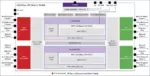
TERAFAB is a $20–25 billion joint venture between Tesla, SpaceX, and xAI, to be built at Giga Texas in Austin, consolidating chip design, lithography, fabrication, memory production, packaging, and testing under one roof—vertical integration no semiconductor company has attempted at this scale, for reasons that will become apparent. The stated production target is chips with an aggregate power draw of one terawatt—roughly fifty times the estimated power consumption of all advanced AI chips currently in production worldwide.
Musk uses power draw as his unit of scale because it is the one metric that translates across wildly different chip architectures, and because it serves his core argument: total US grid capacity runs approximately 0.5 terawatts, making a terawatt of chip power physically impossible to run on Earth. Most of it, he concludes, must go to space. Getting that much compute into orbit means launching roughly 10 million tons per year—approximately 50,000 Starship flights annually, or one every ten minutes. Musk provided no construction or production timeline..
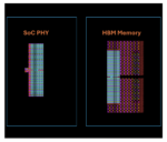
TERAFAB is intended to produce two chip families: AI5, a purpose-stripped inference processor for Tesla vehicles and Optimus robots, with design nearly complete and small-batch production expected later this year; and D3, a space-hardened chip purpose-built for the orbital satellite constellation. Musk has described personal involvement in AI5’s design—the strategic decisions appear to be his; the detailed engineering work is being done by Tesla’s in-house chip team, whose names are not public. The D3 has no disclosed timeline, no foundry assignment, and no published architecture. SpaceX has already filed with the FCC to launch up to one million satellites built around it. The satellites are ready for ordering. The chip is ready for naming.
If launch prices fall to the levels Musk is targeting and TERAFAB delivers at anything approaching its stated capacity, the economics of orbital compute become at least arguable. Space offers effectively unlimited siting, free radiative cooling, and abundant solar power without grid or permitting constraints. In that model, the long-term savings eventually swamp the upfront cost of getting hardware off the ground. The physics are genuine. The execution is another matter.
What Stays on the Ground
Anything with a human or machine waiting on a response. Conversational AI, agentic pipelines, autonomous vehicles, industrial robotics, financial systems, real-time audio and video processing—all require response times that orbital round-trips cannot accommodate. LEO adds 40–80ms of latency before a single computation runs. GEO pushes that past 500ms. For a user waiting on a reply, or a robot waiting on a command, that’s disqualifying. Gravity, it turns out, is not the only thing keeping compute on Earth.
What moves to orbit? Training runs and batch workloads. A model training job that takes days doesn’t care about a 60ms round-trip. Neither does batch inference, large-scale data processing, scientific simulation, or pre-generated content rendering. These are the workloads that consume the most power and are hardest to site on Earth—and they are genuinely good candidates for orbital migration, if someone can build the infrastructure to get them there.
The 80 Percent Problem
Here is where Musk’s headline figure deserves scrutiny. Current data on workload composition suggests the orbital-eligible fraction of global data center compute is closer to 20–30 percent—not 80. The gap between those numbers is not a rounding error. It is the entire argument.
According to McKinsey’s December 2025 data center demand model, total global data center demand in 2025 runs approximately 82 GW, with AI training accounting for 23 GW, AI inference 21 GW, and non-AI workloads 38 GW. [McKinsey & Company] Training—the most straightforwardly orbital-eligible workload—represents roughly 28 percent of the total. Add the latency-tolerant fraction of batch processing and non-AI workloads and you might reach 35–40 percent, generously.
The bigger problem is where growth is headed. Inference will account for roughly two-thirds of all AI compute by 2026, up from about one-third in 2023. [Deloitte Insights] And inference is structurally latency-bound. Inference workloads follow user behavior, and real-time responsiveness is key—which is why inference infrastructure needs to be close to population centers. [Edgecore] That requirement doesn’t dissolve with cheaper launch costs. It doesn’t dissolve at all.
McKinsey projects that by 2030, AI inference will represent more than 40 percent of total data center demand, overtaking non-AI workloads by 2029, while training holds steady at just under 30 percent. [McKinsey & Company] The dominant and fastest-growing category of compute is precisely the one most resistant to orbital migration. Musk’s 80 percent assumes a future where most inference migrates off-planet—which would require either a latency breakthrough that does not appear on any roadmap, or a fundamental restructuring of how AI applications are built that nobody has proposed.
None of this invalidates the core insight. Training workloads are insensitive to latency and can tolerate delays of up to 100 milliseconds between adjacent regions, which already allows hyperscalers to site them in remote, power-rich areas where grid capacity, land, and water are more available. [McKinsey & Company] Orbit is simply the logical extreme of that same siting logic. A more defensible claim might be that orbital compute captures 25–35 percent of global data center demand within the next two decades, concentrated in training and scheduled batch workloads. That is still an enormous market. It is just not the one Musk described in Austin.
The Harder Questions
Thermal management in low earth orbit, radiation hardening at scale, on-orbit servicing, and debris risk remain largely unaddressed in Musk’s public presentation. The D3’s design philosophy—running hotter to shed radiator mass—is elegant engineering thinking. But a chip that hasn’t taped out is not a solution to any of those problems yet. And the launch arithmetic is sobering: 50,000 Starship flights a year is not an engineering challenge, it is a category error relative to anything in the current manifest.
What is real: the terrestrial power constraint driving this vision is genuine and worsening. The semiconductor and systems industries have been quietly watching data center power demand outrun grid capacity for years. Musk is the first person with launch infrastructure, chip design capability, and apparent willingness to spend $25 billion making the orbital alternative credible. That is worth taking seriously, even if the specific numbers are not.
In Austin last week, the conversation shifted. Whether or not TERAFAB delivers on its promises, orbital compute is no longer a thought experiment. That much Musk has accomplished—which is, it should be said, more than most people accomplish in a career.
The rest of the scorecard, however, looks like this: Dojo was cancelled, revived, renamed, and partially absorbed into AI6—all within six months. AI5 was “finished” in July 2025, “almost done” in January 2026, and still not taped out in March. The D3 chip that the entire orbital compute vision depends on has no disclosed design, foundry, or timeline. SpaceX has an FCC filing for a million satellites built around a chip that doesn’t exist yet. And TERAFAB itself has no construction timeline and a price tag that isn’t in Tesla’s capital plan.
Standing in front of all of that, Musk announced the next three projects: megawatt satellites, a lunar factory, and an electromagnetic mass driver on the Moon.
He is, as ever, a man who is always three projects ahead of his last unfinished one.
Also Read:
Silicon Insurance: Why eFPGA is Cheaper Than a Respin — and Why It Matters in the Intel 18A Era
Captain America: Can Elon Musk Save America’s Chip Manufacturing Industry?
TSMC Technology Symposium 2026: Advancing the Future of Semiconductor Innovation