Did we (the analyst) completely underestimate SuperSpeed USB take-off, or is the company tweaking the meaning of “USB 3.0 IP Design-In”? This PRfrom PLDA could be understood as a claiming from the IP vendor that they have achieved the 100[SUP]th[/SUP] design win for their USB 3.0 IP… Let’s try to understand how PLDA can make more design win than the Total Available Market for SuperSpeed IP.
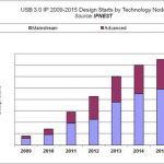
In fact, as an analyst providing “USB 3.0 IP Market Forecast”, I feel very uncomfortable, as the cumulated forecast for 2009, 2010 and 2011 gives 12 + 20 + 59, or 91 ASIC design starts including USB 3.0 IP (sold by an IP vendor). IPNEST thinks we will see Smartphone and Media Tablet supporting USB 3.0 on the market as soon as next year, that USB 3.0 enabled external HDD and SSD are shipping now, and that there will be a second wave of consumer electronics devices to transition, namely the Digital TV, Set-Top-Box, Blue Ray Players to ship in 2012-2013. This means IP sales starting now and continuing in 2012 to allow for a minimum development time. In fact we have built a forecast for USB 3.0 IP sales based on a bottom-up analysis, looking at the different application in every market segment which could transition to USB 3.0, and even more important, we have tried to determine when the IP sales will happen, application by application. The result is a very complete 50 pages document, where you can find this type of information, like the design start evaluation (generating USB 3.0 IP sales) up to 2015:
The first point is that PLDA is not the only vendor selling this IP: Arasan, Evatronix, Faraday, Inventure, NEC (now Renesas), Synopsys and Snowbush are all active on this market. Even if the forecast is wrong by 10% (yes, this can happen!), it’s not possible to see a single company enjoying 100% market share. Especially when reminding that Synopsys has claimed a few weeks ago that they have made 40 USB 3.0 IP design wins, which is rather realistic. First outcome of this investigation; PLDA “design win” does not mean sales of a USB 3.0 IP linked with an ASIC design start. Looks like some design win are for potatoes, when some other are like counting tomatoes. Next question is; which is tomato, which is potato!
Going further in PLDA’ PR, you read that the company is marketing USB 3.0 IP under different form:
- USB 3.0 Host and Device controller IP for implementation in ASIC,
- USB 3.0 Device controller IP for implementation in FPGA,
- USB 3.0 Development boards and kits based on Altera and Xilinx FPGA
Potatoes could be USB 3.0 IP for implementation in ASIC, and tomatoes for implementation in FPGA? Unfortunately not! SuperSpeed USB is a protocol addressing market segment like PC peripheral (External HDD or SSD…), Consumer Electronic (Video Camera…) or Wireless Handset (Smartphone), at least for the time being, until a wider pervasion of the protocol occurs in other segments. Considering the targeted production volumes (several million of units), none of these Application could afford the high ASP value for FPGA devices. We could imagine a scenario where the chip maker decide to validate the concept by targeting a FPGA implementation first, this strategy make sense and is used by chipmakers. But, in this case, they tend to use exactly the same IP than for the ASIC implementation. This would not generate 50 “tomato” design win, as it would mean that PLDA has made 50 “potato” (ASIC) design wins as well, which is very doubtful: how could the challenger in USB 3.0, who was not present on the USB IP market so far could do better than the historical leader? So, the answer is: neither potato, neither tomato! Next question is: what is the vegetable hidden in these 100 design wins?
SuperUSBV6-550 USB 3.0 Development Kit from PLDA
SuperUSBC3-55USB 3.0 Development Kit from PLDA
As I did not want to provide Semiwiki readers with corrupted information, based on my own guess, I simply have asked to PLDA. The vast majority of these 100 design wins have been made by selling FPGA based boards! Because PLDA ‘ Superspeed Controller IP was implemented into the FPGA, PLDA could claim that they have sold, not only the Xilinx or Altera based board, but also the USB 3.0 IP. Every board sale is counting as a design win for the IP! Which is true, when you consider that the customer buying the board could “play” with PLDA’s IP, and interconnect it with his own design. In that sense, PLDA is doing USB 3.0 evangelization. The drawback is that the revenue generated by one of these design wins is in the few $K, when the revenue generated by a SuperSpeed Controller source code IP is in the few $100K! So, it’s likely that these 100 design wins generate far less money than the 40 design wins from Synopsys… The comparison was between potatoes and tomatoes, but the latest was a USB 3.0 enabled FPGA board, not a USB 3.0 IP license for FPGA implementation, the potato still being a SuperSpeed USB IP license for ASIC implementation.
Eric Esteve from IPNEST – Table of Content for “USB 3.0 IP Forecast 2011-2015” available here