RVN! 26 Banner revised (800 x 100 px) (600 x 100 px)

CEO Interview with Aftkhar Aslam of yieldWerx

CEO Interview with Aftkhar Aslam of yieldWerx
by Daniel Nenni on 02-20-2026 at 6:00 am

IMG 9364 3

Aftkhar Aslam is the Co-Founder and Chief Executive Officer of yieldWerx and a semiconductor industry veteran with more than 30 years of experience spanning manufacturing, test engineering, yield management, IP strategy, and enterprise digital transformation.

Under his leadership, yieldWerx has become a trusted data and yield analytics platform supporting semiconductor companies across fab, assembly, test, advanced packaging, photonics, and AI-driven device manufacturing. The platform enables organizations to unify fragmented manufacturing data into scalable, actionable yield intelligence.

Prior to founding yieldWerx, Aftkhar held senior leadership roles at Texas Instruments, where he served as Worldwide Director of Test & Yield Management Solutions & Director of Digital Transformation in the space of Design and Delivery systems and solutions across HW and SW.

He also served as a Director within Accenture’s Industry X (IX) practice, where he advised leading global technology organizations including Intel, GlobalFoundries, Qualcomm, Lam Research, Microsoft, STMicroelectronics, and Skyworks. His consulting work focused on bridging the Design-to-Manufacturing divide — architecting Digital Thread and Digital Twin strategies that connected product design, IP management, manufacturing execution, test, and enterprise systems into unified operational frameworks.

Aftkhar holds patents and possesses deep expertise in intellectual property management and protection. His experience spans semiconductor IP lifecycle governance, secure data architectures, and protecting high-value design assets across complex global supply chains.

Tell us about your company.

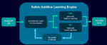
yieldWerx is a semiconductor-focused data and enterprise yield analytics platform. We help manufacturers unify data across fab, assembly, test, inspection, and advanced packaging into a single environment where engineers can extract real insight — not just generate reports.

What makes us different is that we tend to operate where the problems are hardest. We work with highly specialized, niche products and manufacturing flows — whether that’s heterogeneous integration, chiplets, co-packaged optics, MicroLED with billions of pixel-level data points, or silicon photonics requiring optical and electrical correlation. These aren’t simple wafer-yield problems; they’re multi-domain, multi-stage challenges that traditional tools struggle to handle.

We’re purpose-built for semiconductor manufacturing at extreme scale and extreme complexity. Our platform is designed to manage unconventional data models, massive datasets, and deep traceability requirements without breaking performance or usability.

At a high level, we help companies move from fragmented data silos to a connected digital thread — accelerating yield learning, reducing ambiguity, and enabling smarter, faster engineering decisions in some of the industry’s most advanced and specialized product environments.

What problems are you solving?

The biggest problem in semiconductor manufacturing today isn’t lack of data — it’s fragmentation.

Data lives in MES systems, testers, inspection tools, spreadsheets, homegrown databases, and separate analytics platforms. Engineers spend enormous time manually stitching it together before they can even begin root-cause analysis.

We solve that by unifying the data model and enabling cross-domain correlation — electrical + optical, wafer + module, socket + silicon, defect + yield, and so on.

Another major problem is scale. Modern devices generate massive datasets. Traditional tools weren’t designed for billions of data points. Ultimately, we reduce the time from anomaly detection to root cause — and that directly impacts yield, cost, and time-to-market.

What application areas are your strongest?

We’re strongest in environments where complexity is high and data volumes are extreme.

That includes:

  • Advanced packaging (2.5D/3D, chiplets, CPO)
  • Silicon photonics
  • MicroLED and display technologies
  • AI and high-performance compute devices
  • Automotive and high-reliability semiconductor manufacturing

Anywhere there’s multi-stage manufacturing with complex traceability requirements — that’s where we add the most value.

What keeps your customers up at night?

Three things:

  1. Yield ramp speed — especially for new technologies. Every week of delay is expensive.
  2. Escapes or overkill at test — failing good parts or shipping marginal ones.
  3. Lack of traceability when something goes wrong.

They worry about whether they truly understand where yield loss is originating — is it the wafer, the packaging step, the bonding process, the socket, the test program?

If the answer takes weeks to figure out, that’s a problem. Our goal is to make that answer visible in hours or days.

What does the competitive landscape look like and how do you differentiate?

There are traditional yield tools, BI tools, and homegrown systems.

Traditional yield tools often focus on wafer-level analysis but struggle with cross-domain traceability. BI tools are flexible but require heavy customization and don’t inherently understand semiconductor manufacturing.

We differentiate in three ways:

  1. Semiconductor-native data model — we understand wafers, panels, bonding, pixel maps, optical lanes, serialized modules.
  2. Extreme scalability — billions of records without performance degradation.
  3. Closed-loop capability — we don’t just visualize data; we enable correlation across design, manufacturing stages to drive actionable decisions.

We’re not just another dashboard — we’re the infrastructure layer for yield intelligence.

What new features or technology are you working on?

We’re expanding heavily into:

  • Pixel-level and device-level analytics for MicroLED and advanced displays
  • Optical + electrical unified analysis for photonics and CPO
  • Advanced spatial analytics and pattern recognition
  • AI-assisted anomaly detection and predictive yield modeling from the start of design
  • Deeper integration with test hardware and equipment for closed-loop optimization

We’re also strengthening genealogy and digital-thread capabilities to support next-generation packaging and heterogeneous integration.

The industry is moving toward system-level understanding, not just wafer-level — and that’s where we’re investing.

How do customers normally engage with your company?

Most engagements start with a specific pain point — slow yield ramp, fragmented data, lack of traceability, or scaling a new technology.

We typically begin with a focused pilot or proof-of-value around a real manufacturing dataset. Once customers see how quickly we can unify and analyze their data, the engagement expands into a broader enterprise deployment.

We also work closely with equipment providers, OSATs, and ecosystem partners, because yield today is collaborative — not isolated.

At the end of the day, we’re a long-term partner. Once we’re embedded in the manufacturing data flow, we become part of the operational backbone.

CONTACT yieldWerx

Also Read:

CEO Interview with Elad Raz of NextSilicon

VSORA Board Chair Sandra Rivera on Solutions for AI Inference and LLM Processing

CEO Interview with Dr. Raj Gautam Dutta of Silicon Assurance


Intelligent Networks: Power, Reliability, and Maintenance in Telecom — Webinar Preview

Intelligent Networks: Power, Reliability, and Maintenance in Telecom — Webinar Preview
by Daniel Nenni on 02-19-2026 at 2:00 pm

Intelligent Networks semiwiki ads v7 400x400px

The upcoming webinar “Intelligent Networks: Power, Reliability, and Maintenance in Telecom” will focus on how telecommunications networks are adapting to growing demands for efficiency, resilience, and scalability. As telecom operators expand 5G deployments, integrate cloud-native architectures, and prepare for AI-driven services, the need for intelligent, automated network management has never been greater. This webinar aims to explore how intelligence embedded across the network can help operators address three critical challenges: power consumption, network reliability, and maintenance optimization.

One of the key topics to be addressed is power management in modern telecom networks. With increasing network densification, edge deployments, and higher-capacity equipment, energy usage has become a major operational and financial concern. The webinar will examine how intelligent networks can leverage real-time data, analytics, and automation to optimize power usage across sites and network elements. By aligning power consumption with traffic demand and operational conditions, operators can reduce energy waste, lower operational expenses, and support sustainability goals without compromising performance.

The webinar will also highlight reliability as a core requirement for next-generation telecom services. As networks support mission-critical applications, ranging from emergency communications to industrial automation, downtime and service degradation are no longer acceptable. Speakers are expected to discuss how intelligent networking technologies enable proactive reliability strategies, moving beyond traditional reactive fault management. Topics will include the use of advanced telemetry, AI-driven anomaly detection, and predictive analytics to identify potential failures before they impact service, helping operators maintain high availability and consistent quality of experience.

Another major focus of the session will be the evolution of maintenance practices in telecom environments. Conventional maintenance models, based on fixed schedules or manual inspections, can be inefficient and costly, particularly in large-scale, geographically distributed networks. The webinar will explore how intelligent networks support predictive and condition-based maintenance approaches. By continuously monitoring network health indicators such as power systems, cooling infrastructure, and hardware performance, operators can anticipate issues and intervene at the optimal time. This approach reduces unnecessary site visits, minimizes service disruptions, and extends the lifespan of critical assets.

Automation and orchestration are expected to be recurring themes throughout the discussion. As telecom networks grow in size and complexity, manual management becomes increasingly impractical. The webinar will examine how intelligent network platforms can automate routine tasks such as fault correlation, power optimization, and service recovery. Centralized visibility and intelligent orchestration enable operators to respond faster to issues, improve operational efficiency, and scale their networks with confidence.

In addition, the webinar will touch on network resilience and security, recognizing that reliability is not limited to physical infrastructure or power availability. As networks become more software-driven and interconnected, they also face greater exposure to cyber threats. Intelligent networks can enhance resilience by identifying abnormal behavior, supporting rapid mitigation, and maintaining service continuity in the face of both physical and digital disruptions.

Overall, “Intelligent Networks: Power, Reliability, and Maintenance in Telecom” is positioned to provide valuable insights into how intelligence, automation, and data-driven decision-making are shaping the future of telecom operations. By addressing power efficiency, reliability, and maintenance as interconnected challenges, the webinar will offer a holistic perspective on building networks that are more sustainable, resilient, and prepared for future demands. For telecom operators, vendors, and industry stakeholders, the session promises to outline practical strategies and emerging best practices for navigating the next phase of network evolution.

REGISTER HERE

Also Read:

Accelerating NPI with Deep Data: From First Silicon to Volume

Failure Prevention with Real-Time Health Monitoring: A proteanTecs Innovation

Thermal Sensing Headache Finally Over for 2nm and Beyond


Custom IC Design using Additive Learning

Custom IC Design using Additive Learning
by Daniel Payne on 02-19-2026 at 10:00 am

Additive learning engine

Custom IC design has demanding technical requirements to produce accurate simulation results for timing and power analysis in the shortest run times. EDA vendors have been rushing to use AI and ML technology to meet these analysis requirements. I attended a webinar from Siemens on accelerating iterative design cycles with Solido additive learning techniques to understand their approach to benefit custom IC designers.

Mohamed Atousa, Product Management Manager at Siemens started with an overview of their custom IC platform with tools spanning from schematic capture, variation-aware design, physical layout, library characterization, IP QA, and SPICE simulation to generative and agentic AI.

Within the Solido Design Environment are multiple analysis tools and the focus of this webinar was on the additive learning features used in PVTMC Verifier and the High-Sigma Verifier tools to achieve a 3X to 20X speed-up on incremental and iterative runs.

High-quality IC designs require variation-aware verification flows, yet the traditional Monte Carlo simulation methods run too slowly, but using extrapolation techniques cannot find outliers or model non-Gaussian behavior, and most simulation jobs are iterative. Making minor changes in a design or PDK require re-verification, creating verification flows that are too time consuming.

The new AI technologies enable SPICE-accurate variation-aware verification that is much faster than previous approaches. In the Solido PVTMC Verifier there is full coverage verification across PVT corners plus Monte Carlo, showing speedups of 2X to 10X, allowing it to find outliers that other methods can’t. AI used in Solido High-Sigma Verifier is able to produce 6-sigma yield verification in only thousands of circuit simulations, resulting in speed-ups from 1,000X to a Billion X faster than brute-force, all while maintaining SPICE accuracy.

Jayne Alexander, Technical Product Manager at Siemens talked next about how additive learning technology retains and reuses AI models to speed-up iterative workflows by 3X – 20X. In a traditional workflow it is common to verify a design, then have to re-verify because of changes in: PDK revision, transistor sizing, simulator versions, adding more corners, etc. With the new iterative workflow there is still the first run, but subsequent verification run times are much reduced as previous results are stored for re-use.

With the Solido Additive Learning Engine you experience accurate verification results every time, automatically. Here’s the internal flow chart to achieve this benefit.

This additive learning technology retains and reuses AI models from previous jobs to speed up iterative runs, making it fast and accurate while automating the process, while requiring no user-input or AI knowledge for the tool users. Under the hood there is an AI datastore that is designed to be light-weight and optimized, supporting multiple users at once, all while using small disk space.

From Microchip we heard from Amit Bansal, Technical Staff Engineer and their old iterative design process was taking 20-30 days. They ran PVTMC Verifier on bandgap reference circuits and RC oscillators, with and without Additive Learning (AL). For the bandgap reference circuit they made a design change on the pre-layout netlist then verified at 3 sigma across 21 PVT corners. The results were 3.7X fewer simulations, 4.1X wall clock speedup:

  • Base run – 885 simulations, 2hr 16min

  • AL off – 1,170 simulations, 3hr 24 min

  • AL on – 315 simulations (3.7X), 49min (4.1X)

In the RC oscillator example they changed the trim cap value in the post-layout netlist then verified at 3 sigma across 1 PVT corner. More impressive results with 20X fewer simulations, 18X wall clock speedup:

  • Base run – 300 simulations, 14 hr 16 min

  • AL off – 300 simulations, 11hr 40min

  • AL on – 15 simulations (20X), 39min (18X)

At DAC 2025 Microchip and Siemens presented their results in the Poster Gladiator Competition and won.

Summary

With verification times taking too long for custom IC designs with many iterations there has to be a better way than using brute-force Monte Carlo simulations and then waiting for answers. Thanks to AI-powered features like additive learning, the Solido tools have been shown to reduce the number of simulations by producing faster analysis answers, all while maintaining accuracy. Users can be productive quickly with no learning curve or AI expertise required, it’s out of the box easy with minimal to no user input required.

Watch the archived webinar online here.

Related Blogs


SiFive’s AI’s Next Chapter: RISC-V and Custom Silicon

SiFive’s AI’s Next Chapter: RISC-V and Custom Silicon
by Daniel Nenni on 02-18-2026 at 2:00 pm

AI’s Next Chapter RISC V and Custom Silicon

In the rapidly evolving world of artificial intelligence and semiconductor design, open-standard processor architectures are gaining unprecedented traction. At the center of this shift is SiFive, a company founded by the original creators of the RISC-V ISA, which champions an open, extensible, and license-free alternative to proprietary architectures like x86 and Arm. A webinar titled “SiFive AI’s Next Chapter: RISC-V and Custom Silicon” encapsulates the company’s vision for how RISC-V and tailored silicon platforms will power the next wave of AI innovation, from edge devices to large-scale data centers.

The Strategic Importance of RISC-V for AI

At its core, RISC-V is a modular ISA that lets designers choose only the instruction subsets they need, and extend the base set with custom extensions suited to their applications. This openness dramatically reduces barriers to entry and enables highly specialized designs that can be optimized for power, performance, and area, crucial for AI and machine learning workloads. Unlike closed ISAs where licensing fees and fixed capabilities constrain flexibility, RISC-V allows custom silicon to be tailored from the ground up for specific AI use cases, from inference at the edge to large model training in the cloud.

A webinar on this subject would likely begin by framing why open ISAs are now receiving serious attention: as AI workloads grow in size and complexity, traditional CPU designs can become bottlenecks. Custom silicon chips designed with specific AI functions built directly into the silicon can accelerate key operations like matrix multiplication, tensor processing, and low-precision arithmetic. RISC-V’s flexible ISA makes it easier to implement such features efficiently. Moreover, as traditional leaders in processor design (like Arm) face increasing licensing constraints or strategic shifts, an open foundation like RISC-V offers an attractive alternative for companies wanting to future-proof their hardware roadmaps.

Custom Silicon: Tailoring Processors to AI Workloads

The “custom silicon” part of the webinar title refers to the creation of chips specifically architected for particular AI demands. Rather than using generic CPUs and off-the-shelf components, custom silicon can embed accelerators, optimize memory hierarchies, and integrate unique instruction extensions that speed up AI computations at lower energy consumption. In a field where efficiency and performance per watt are critical, these gains matter.

For example, SiFive’s own products, such as its Intelligence and Performance families, integrate vector and matrix computation units into RISC-V CPUs, allowing these cores to act as accelerator control units that manage AI workloads more efficiently than general-purpose processors alone. This approach drastically reduces overhead and can enable better AI performance on devices ranging from autonomous sensors to cloud servers.

Another important theme is ecosystem enablement. A custom silicon strategy only succeeds if a robust toolchain, including compilers, libraries, and runtime support, enables developers to target these designs. SiFive and partners have been building out support for major AI frameworks and compilers so that developers can deploy models efficiently on RISC-V platforms without sacrificing software compatibility or developer productivity.

Industry Collaboration and Co-Design

Webinars on RISC-V often include discussions about ecosystem partnerships and co-design approaches. For instance, recent announcements highlight collaborations between SiFive and companies such as NVIDIA, integrating technologies like NVLink to enable coherent, high-bandwidth CPU-to-accelerator communication, a major innovation for AI data centers where latency and bandwidth can dramatically impact scaling and throughput.

Similarly, the adoption of RISC-V by other ecosystem players, including major cloud providers and AI accelerator developers, underscores a broader industry shift toward heterogeneous computing architectures where CPUs, GPUs, and custom accelerators work in concert. These partnerships demonstrate how open ISAs and custom silicon are no longer niche, they are becoming central to next-generation AI infrastructure design.

Takeaways for Developers and Architects

A webinar like “SiFive AI’s Next Chapter: RISC-V and Custom Silicon” serves multiple audiences: hardware architects seeking insights on cutting-edge silicon design; software developers interested in how AI workloads can be optimized on RISC-V; and industry strategists evaluating open standard architectures against incumbent designs. Key takeaways would include:

  • How RISC-V’s modular ISA facilitates tailored processor designs for specific AI models and workloads.
  • The advantages of custom silicon in boosting performance and efficiency for AI machine learning functions.
  • Case studies or technical deep dives showing how SiFive’s RISC-V IP can be applied across edge, embedded, and data center use cases.
  • A look into emerging collaborations and ecosystem developments that broaden the practical applicability of RISC-V.

Bottom Line: This webinar represents not just a technical briefing but a reflection of a broader industry narrative: open, customizable hardware built on RISC-V is steadily transforming the AI computing landscape. As AI models continue to grow in complexity and deployment scenarios diversify, processor architectures that offer flexibility, efficiency, and extensibility, hallmarks of RISC-V and custom silicon , are set to play a foundational role in the future of AI.

Also Read:

SiFive to Power Next-Gen RISC-V AI Data Centers with NVIDIA NVLink Fusion

Tiling Support in SiFive’s AI/ML Software Stack for RISC-V Vector-Matrix Extension

RISC-V Extensions for AI: Enhancing Performance in Machine Learning


Smarter IC Layout Parasitic Analysis

Smarter IC Layout Parasitic Analysis
by Daniel Payne on 02-18-2026 at 10:00 am

ParagonX flow

IC layout parasitics dominate the performance of custom digital, analog and mixed-signal designs, so the challenge becomes how to identify the root causes and to quantify the effects of parasitics during early design stages. The old method of iterating between layout, extraction, SPICE simulation, followed by manual debug and analysis is just too slow and error prone to be relied upon. A smarter approach has been developed with an EDA tool called ParagonX from Synopsys, so I attended a recent webinar to become more informed. ParagonX came from start-up Diakopto which was acquired by Ansys, then Synopsys acquired Ansys.

Rob Dohanyos of Synopsys opened up the webinar with an overview of ParagonX and then most of the time was spent in a live demo, something kind of rare with EDA vendors. The ParagonX tool can be used by a circuit designer to analyze, debug, visualize and even optimize their IC layout parasitics for any technology node and any circuit design style. Typical users of the tool are designing high-speed or high-precision circuits, like: SERDES, optical transceivers, ADC, DAC, SRAM, clocks. Parasitic sensitive designs also benefit from this analysis: Analog, power nets, PMICs, ESD networks, guard rings. Smaller nodes benefit even more from ParagonX, all the way down to 3nm. Instead of spending weeks and months debugging parasitic effects, a designer can reduce that time to hours or minutes.

Circuit designers and layout engineers will find the new tool to be easy to use out of the box, with quick run times, while providing insights to any problem areas. Here’s where ParagonX fits into your existing design and layout flow:

This tool can accept netlists that are hundreds of gigabytes in size and analyze nets that have hundreds of millions nodes or resistors, all made possible through it’s own binary netlist database. Users can expect fast netlist loading for top-hierarchy analysis, including power net analysis all while using the interactive GUI. There are six basic analysis features in ParagonX:

Invoking the tool brought up a GUI with choices grouped by analysis features, then they loaded a netlist in a few seconds. All nets could be traversed with a hierarchical widget, plus searching for nets with wildcards made it fast to find a specific net. Point to point (P2P) resistance was shown by selecting start and end points, and then the resistance contributions were displayed by layer type and percentage contribution.

The top four layers had the most resistance, so next they showed sensitivity analysis with visualization of the layout by color-coded resistance.

Each of the many functions in the ParagonX tool are actually Pythons scripts that you can customize to fit your own analysis needs. From the command line of the tool you can see each script being used for a particular function. A function called Rview shows the resistance to all points on one net, and this got 1,000 times faster in the latest tool release. Rob ran Rview on a sample net VIN, showing 240 instance pins with a resistance distribution of 100 to 450 ohms.

Next in the demo the capacitive coupling on a single net was run on net VIN and all aggressor nets, showing that VSS had the most coupling from VIN to diffusion. Metal 3 had the highest coupling on VIN with CLOCK S. Users can tell which nets and layers are causing the most coupling, both numerically and visually.

RC delay was another function demonstrated with a start point of VIN to all instance points, then a device characterization file was generated for use with a specific SPICE tool. Sensitivity of RC delay to parasitics was the next function displayed using a rainbow of colors.

The net matching function was run on a differential pair, VIN and VIP, where the user set the matching criteria and simulation results showed layout areas in red that were not matching, while areas in green were matching properly. Several other functions were demonstrated: Layout Parasitic Screener, What-if analysis, victim noise analysis, glitch analysis.

Summary

Circuit and layout designers now have a much smarter way to quickly analyze IC layout parasitics, find the root cause and even begin to optimize their designs by using the ParagonX tool in their flow. This really is a new EDA tool category and will benefit custom-digital, analog and mixed-signal design projects.

Watch the archived webinar online.

Related Blogs


Improving Retrieval Accuracy in AI

Improving Retrieval Accuracy in AI
by Bernard Murphy on 02-18-2026 at 6:00 am

Agentic RAG expert

While there are big ambitions for virtual engineers and other self-guiding agentic applications, today estimates show 83-90% of AI inferences are for internet searches. On a related note, chatbots are now said to account for nearly 60% of internet traffic. Search and support are the biggest market drivers for automation and unquestionably have improved through AI automation. Search gets closer to what you want in one pass. Chatbots also depend on retrieving domain-specific information following a question. In either case, RAG – retrieval augmented generation – plays an important role in finding the most relevant sources for a search or chat response.

Or so you hope. My experience is that the RAG results I get in a basic search/question are most useful for simple (one-part) questions in areas where I have no expertise. The more expertise I have or the more complex my question, the less useful I find the response. I can do somewhat better by adding context (You are an expert in … My question is …). Asking for citations also helps. But even these tricks don’t always work. The problem is that RAG as originally conceived (2020) has limitations. I thought it would be interesting to look at advances in this field, for variety looking from a business perspective and a healthcare perspective. In AI, it seems that our needs and priorities are not so different.

A business perspective from Elastic and Cohere

Target applications here cover a wide range in business: finance, public sector, energy, media, etc. I found this webinar which presents a combination of these two technologies with particular emphasis on RAG, the basics, challenges, and advances.

First, a quick note on RAG. LLMs are trained on publicly accessible corpora. RAG training derives information from separate and typically internal proprietary sources: PDFs, spreadsheets, images, etc. This information is chunked in some manner (eg. paragraphs in PDF text) and encoded as vectors based on similarity (scalar products of vectors, so related objects are close and unrelated objects are not). Chunks in training data must be expert (human) labeled.

Retrieval then uses a mix of keyword matching and similarity-based search to develop a top-ranked set of responses to your question. RAG is more accurate in retrieval than a general-purpose LLM because it can exploit semantic understanding based on similarity matching between a query and labeled training data.

So far this is naive RAG, with known limitations. These include struggles where the answer needed may require wider understanding of a source, or multiple sources, or the question asked has multiple clauses and requires sequential reasoning.

You know what’s coming next: agentic RAG, also called advanced-RAG. To address these limitations a system must develop a plan of attack, do multiple hops of reasoning, and self-reflect/verify after each step, potentially triggering rework. This is what agentic does. As soon as a question/request becomes even moderately complex, resolution must turn agentic, even in RAG. Tools used to support such agentic flows in business applications might be Microsoft Office, CRM, or SQL databases.

For completeness, a further advance you may find is modular RAG. These systems allow for more building block approaches to blend retrieval and refinement in structuring pipelines.

A healthcare perspective from Kent State and Rutgers

Here I draw on a long but very interesting paper. The authors suggest the following as key applications in healthcare: diagnostic assistance by retrieving information on similar cases; summarizing health records and discharge notes; answering complex medical questions; educating patients and tailoring responses to user profiles; matching candidates to clinical trials; and retrieving and summarizing biomedical literature, especially recent literature, in response to a clinical or research query.

The authors note a range of challenges in retrieving information. Obviously such a system must handle a wide range of data types (modalities), from doctor notes to X-rays, EKG traces, lab results, etc. They must also contend with a wide range of potentially incompatible health record sources, some with technically precise notes (myocardial infarction), some less precise (heart attack). Users face challenges in understanding the credibility of sources (media health articles, versus Reddit, versus respected journals in a field) and how these contribute to ranking conclusions. Familiar challenges even in our field.

There is a longer list from which I’ll call out one widely relevant item: the need to continuously update as new research, drugs and treatments emerge, also need to deprecate outdated sources. In a medical context the authors suggest that manual updates would be too slow and error-prone and that any useful RAG system for their purposes must build continuous update into the system.

They look at tradeoffs between the three RAG architectures mentioned earlier (naive, advanced, and modular). They find naive RAG easy to setup and use, though for their purposes too noisy and risky for high-stakes scenarios. Advanced RAG is more promising in diagnostic support and EHR summarization, striking a balance between factual grounding and speed, but requires significant compute resource (presumably an on-prem datacenter). This method looks most ready today for clinical use, at least in hospitals and large clinics. They see modular RAG as interesting for ongoing research, though training and resource costs make it impractical to consider for near-term deployment.

Relevance to design automation

Accuracy is critical for technical support in our domain, whether internal or external. Our users are very knowledgeable and intolerant of beginner-level suggestions. Experiences above suggest that advanced/agentic RAG may be the most appropriate method to deploy support here.

That guidance should aim to avoid mistakes made in some ambitious all-AI rollouts (Klarna customer support for example). These certainly should include emphasis on “don’t know” for suggestions with low support, explainability for top candidate response offered, and methods to escalate to a human expert when the bot is uncertain. I am starting to see some of this in general customer support.

Meantime, agentic RAG can make a big difference in productivity and user satisfaction for in-house and external users. Most of us would prefer to explore on our own supported by effective agentic RAG, only turning to a human expert when we’re not making progress. That’s technology worth supporting.

Also Read:

Bronco Debug Stress Tested Measures Up

TSMC and Cadence Strengthen Partnership to Enable Next-Generation AI and HPC Silicon

How Memory Technology Is Powering the Next Era of Compute


Ceva IP: Powering the Era of Physical AI

Ceva IP: Powering the Era of Physical AI
by Daniel Nenni on 02-17-2026 at 2:00 pm

Ceva IP Powering the Era of Physical AI

Artificial intelligence is rapidly moving beyond the digital domain and into the physical world. From autonomous robots and smart factories to intelligent vehicles and connected consumer devices, AI systems are increasingly expected to perceive their surroundings, make real-time decisions, and act on them instantly. This shift marks the rise of Physical AI, a new generation of intelligence that combines sensing, connectivity, and on-device inference. At the heart of this transformation is Ceva IP, a leading provider of semiconductor and software intellectual property that enables Physical AI at the edge.

Physical AI differs from traditional cloud-centric AI in a fundamental way. Rather than relying on remote servers to process data, Physical AI systems operate directly on the device. They gather data from sensors such as cameras, microphones, radar, and motion detectors, analyze it locally using AI inference engines, and respond in real time. This approach is essential for applications where latency, power efficiency, reliability, and privacy are critical. Ceva’s technology portfolio is purpose-built to address these exact requirements.

Ceva’s role in Physical AI begins with connectivity, a foundational pillar for intelligent devices. The company offers a comprehensive suite of wireless IP solutions, including Bluetooth, Wi-Fi, ultra-wideband, and cellular technologies. These connectivity solutions allow devices to communicate seamlessly with other machines, infrastructure, and ecosystems while maintaining low latency and high reliability. In Physical AI systems, fast and robust wireless communication ensures that sensor data, control signals, and AI-driven decisions flow without interruption, even in complex or dynamic environments.

Equally important is sensing and sensor fusion, another core strength of Ceva IP. Physical AI systems rely on multiple sensors to understand the real world accurately. Ceva provides DSP architectures and software frameworks optimized for handling multimodal sensor data. By efficiently combining inputs from vision, audio, motion, and radar sensors, Ceva-powered systems gain a richer, more contextual understanding of their surroundings. This capability is crucial for applications such as robotics, advanced driver-assistance systems (ADAS), and industrial automation, where precise perception directly impacts safety and performance.

At the center of Physical AI lies on-device inference, and this is where Ceva’s neural processing technologies play a decisive role. Ceva’s AI and neural network IP solutions are designed to deliver high performance at ultra-low power, enabling complex AI workloads to run directly on edge devices. These inference engines support a wide range of machine learning models, from classical AI algorithms to modern deep learning networks. By performing inference locally, devices can respond instantly to real-world events without depending on cloud connectivity, while also protecting sensitive data.

One of Ceva’s key differentiators is its system-level approach. Rather than offering isolated components, Ceva provides an integrated IP ecosystem that allows semiconductor designers to build complete Physical AI platforms. Connectivity, sensing, and inference IP blocks are designed to work together efficiently, reducing integration complexity and accelerating time to market. This modular and scalable approach enables customers to tailor solutions for diverse applications, from tiny battery-powered IoT devices to high-performance automotive and industrial systems.

The impact of Ceva IP is already visible at scale. Ceva technologies have been deployed in tens of billions of devices worldwide, underscoring the company’s influence across consumer, automotive, industrial, and mobile markets. As the demand for smarter, more autonomous systems continues to grow, Physical AI is becoming a defining trend in the semiconductor industry.

Bottom line: Ceva IP is powering the era of Physical AI by providing the essential building blocks that allow machines to sense, connect, think, and act in the real world. By enabling real-time intelligence at the edge, Ceva is helping bridge the gap between digital computation and physical interaction—unlocking a new generation of responsive, efficient, and intelligent devices.

CONTACT CEVA-IP

Also Read:

Ceva-XC21 Crowned “Best IP/Processor of the Year”

United Micro Technology and Ceva Collaborate for 5G RedCap SoC and Why it Matters

Ceva Unleashes Wi-Fi 7 Pulse: Awakening Instant AI Brains in IoT and Physical Robots


Accelerating Static ESD Simulation for Full-Chip and Multi-Die Designs with Synopsys PathFinder-SC

Accelerating Static ESD Simulation for Full-Chip and Multi-Die Designs with Synopsys PathFinder-SC
by Kalar Rajendiran on 02-17-2026 at 10:00 am

SNPS PathFinder SC ESD Verification

As analog and mixed-signal designs become increasingly complex, parasitic effects dominate both design time and cost, consuming 30–50% of engineers’ effort in debugging and reanalyzing circuits. Addressing these multiphysics effects requires early verification strategies and reliable simulation solutions. Modern verification must extend beyond traditional RC parasitics to encompass inductance, RF interactions, voltage drop, RDS(on) effects, thermal behavior, signal integrity, photonics, and electrostatic discharge (ESD).

Synopsys recently hosted a webinar on ESD verification for full-chip and multi-die designs using its PathFinder-SC platform. The session was presented by Peter Tsai, Product Manager; Marc Swinnen, Product Marketing Manager; and John Alwyn, Product Specialist. It provided a detailed look at PathFinder-SC’s capabilities in addressing modern ESD verification challenges, highlighting workflows for early-stage validation, full-chip and multi-die simulation, and layout-driven debugging. The session emphasized effective protection circuits, bump-to-bump, bump-to-clamp and clamp-to-clamp discharge paths, and adherence to foundry-certified thresholds for voltage, current, and electromigration limits.

Synopsys PathFinder-SC Overview

PathFinder-SC enables early ESD verification through cell-based modeling of discharge circuits derived from GDS, OASIS, DEF, and LEF data. This approach allows potential reliability issues to be identified well before full layout completion. Its scalable architecture, powered by the Seascape distributed computing platform, supports simulations of full-chip and multi-die designs with billions of nodes.

By leveraging RedHawk-SC’s certified extraction and electromigration engines, PathFinder-SC ensures that effective resistance and current density checks comply with foundry guidelines. This guarantees that discharge paths, metal routing, and protection circuits can safely handle ESD currents. Layout-driven debugging allows engineers to trace shortest-path resistances, visualize current density flows, and pinpoint potential failure points.

Multi-scenario simulations that include variations in bump placement, clamp types, and extraction corners help optimize design robustness. PathFinder-SC also extends verification from the die to the package and board level, incorporating package netlists and compact impedance models to ensure end-to-end reliability.

Technical Capabilities and Workflows

PathFinder-SC supports static ESD simulations, including effective resistance and current density checks along intended discharge paths. It verifies protection circuits such as primary and secondary diodes, clamps, and cross-domain devices, ensuring that ESD currents safely exit through the nearest bump without damaging functional circuits. When discharge paths are poorly routed or have insufficient metalization, unintended paths may form, potentially causing latent device damage. PathFinder-SC detects these weaknesses early, enabling designers to optimize layouts before fabrication.

Simulation workflows include design netlist analysis, physical verification, static resistance and current density simulations, and dynamic simulations. Using schematic and layout checks, PathFinder-SC identifies ESD devices, verifies connections, and ensures compliance with foundry guidelines. Static simulations measure effective resistance and current density along partial or full discharge paths, while dynamic simulations assess peak stress voltages and currents in protection circuits. These analyses enable robust verification of bump-to-bump, bump-to-clamp, and clamp-to-clamp paths, including multi-die interposer connections.

Distributed processing via Seascape allows large designs to be simulated efficiently. Tasks such as geometry processing, resistance extraction, zap simulations, and result aggregation are parallelized across hundreds of CPU cores or cloud workers. PathFinder-SC can handle designs with hundreds of thousands of bumps, tens of thousands of protection devices, and multiple dies, completing workflows in hours rather than days. Sensitivity analysis and shortest-path resistance tracing allow engineers to pinpoint high-resistance segments and electromigration hotspots for targeted optimization.

The tool’s view-based architecture supports simulation of multiple variations in bump placement, clamp types, and extraction corners. Each view executes workflows such as RC extraction, clamp identification, and zap simulations, with results stored in a distributed database for analysis. Users can query the database, visualize current density and electromigration maps, and browse resistance check results for full-chip or multi-die designs. Compact impedance modeling and detailed standard parasitic format (DSPF) stitching allow transient simulations of ESD events, linking die-level and package-level effects.

Performance Insights

Performance metrics shared during the webinar demonstrated PathFinder-SC’s ability to handle very large designs efficiently. Full-chip SoCs and multi-die stacks with millions of nodes, tens of thousands of clamps, and hundreds of thousands of bumps were simulated using distributed workers.

For example, a multi-die 3DIC design with 168,000 protection diodes and 144 clamps completed clamp-to-clamp and bump-to-clamp resistance checks in under 14 hours using 80 CPUs. Current density simulations for a 5nm SoC with around 163,000 PG bumps finished in about 37 hours using 50 CPUs. A very large interposer layout covering 24 cm × 18 cm, with over 500,000 nets and 163 million geometry shapes, completed extraction and design modeling in 47 hours using hundreds of cores. These examples demonstrate that PathFinder-SC scales to extreme design sizes without compromising accuracy or speed.

Summary

The webinar highlighted that ESD events can occur throughout a chip’s lifecycle and ESD verification is especially critical in advanced packaging technologies such as chiplets and 3D ICs. For reliability engineers, physical design engineers, SoC architects, packaging and 3DIC engineers, and others responsible for ESD protection, the session offered in-depth insight into PathFinder-SC’s capabilities. The presenters shared practical workflows, performance statistics, and real-world examples, with actionable guidance for integrating ESD verification into modern design flows. From pre-LVS verification to final signoff, PathFinder-SC helps teams accelerate design completion, mitigate risk, and ensure robust ESD protection in complex, advanced-node chips.

You can watch the entire webinar here.

Also Read:

Podcast EP330: An Overview of DVCon U.S. 2026 with Xiaolin Chen

2026 Outlook with Abhijeet Chakraborty VP, R&D Engineering at Synopsys

Advances in ATPG from Synopsys


A Century of Miracles: From the FET’s Inception to the Horizons Ahead

A Century of Miracles: From the FET’s Inception to the Horizons Ahead
by Daniel Nenni on 02-17-2026 at 6:00 am

From the FET’s Inception to the Horizons Ahead

The Field-Effect Transistor (FET), a cornerstone of modern electronics, marks its centennial in 2025, tracing back to Julius Edgar Lilienfeld’s groundbreaking invention in 1925. Born in 1882 in what is now Lviv, Ukraine, Lilienfeld was a prolific physicist who earned his PhD from Berlin University in 1905. His early work at Leipzig University focused on vacuum conduction, contributing to X-ray tubes and even collaborating with Count Ferdinand von Zeppelin on dirigibles. A friend of Albert Einstein, Lilienfeld relocated to the United States in 1927 to defend his X-ray patents, eventually directing research at Ergon Laboratories in Malden, Massachusetts. There, he explored electrolyte interfaces and semiconductors, leading to his FET patents. Retiring to St. Thomas in 1935 due to allergies, he continued research until his death in 1963 at age 81.

Lilienfeld’s FET aimed to replace bulky vacuum tubes, invented in 1906 by Lee De Forest for wireless communication. Vacuum tubes controlled electron beams easily via grid potential in a vacuum. However, semiconductors posed challenges: abundant charges made current control by a gate electrode nearly impossible. Lilienfeld proposed structures like a MESFET in 1925 using p-type semiconductors with Schottky contacts and a MOSFET in 1928 with an aluminum oxide insulator on copper sulfide.

From 1925 to 1960, FET development stalled with a “hopeless period.” Materials like Cu2S and Cu2O were poor choices, semiconductor purity was abysmal, and foundational physics and technologies were lacking. Progress accelerated around 1940 when silicon was refined for military radar detectors, achieving 99.8% purity via thermal processes. This led to Russell Ohl’s accidental discovery of the pn junction in 1940, separating p-type (boron) and n-type (phosphorus) impurities, enabling photovoltaic and rectification effects.

Key theoretical advances followed. In 1938, Walter Schottky described inversion and depletion layers at metal-semiconductor junctions. Heinrich Welker proposed an inversion layer channel in 1945, noting its thinness for easy gate control and low scattering in depletion regions. By 1953, Walter Brown and William Shockley demonstrated FET operation using a back-gate structure on germanium, incorporating pn junctions for source/drain isolation.

The 1947 invention of the point-contact transistor by John Bardeen and Walter Brattain, followed by Shockley’s bipolar junction transistor (BJT) in 1948, shifted focus temporarily. BJTs benefited from 1950s technologies like silicon crystal pulling, impurity doping, photolithography, ion implantation, and epitaxial growth—processes essential for FETs too, but MOSFETs couldn’t be fabricated without them.

Interface instabilities plagued early MOSFETs, with charges like fixed oxide, trapped, mobile ionic, and interface states causing drift until resolved around 1969. This breakthrough enabled mass production of LSIs. Intel’s 1101 256-bit SRAM (1969) and 1103 1k-bit DRAM (1970) featured over 1,000 MOSFETs, using 8-10 µm rules and multiple voltages. The 1971 Intel 4004, the first microprocessor, integrated 2,300 pMOSFETs at 10 µm, designed by Federico Faggin, Masatoshi Shima, and others.

Robert Dennard’s 1974 scaling scheme revolutionized downsizing: reducing dimensions and voltages by factor K (typically 0.7 every 2-3 years) maintained power density while boosting speed and density. Over 25 generations from 1964’s 20 µm to 2025’s 2 nm, this yielded nanoelectronics, transitioning from PMOS/NMOS to CMOS, bulk to FinFET/GAA structures.

By 2025, line widths approach 10 nm limits—practical (demerits outweigh benefits), direct-tunneling (~3 nm), and atomic (~0.3 nm). Memory cells rival influenza virus sizes; chips hold 100 billion transistors, wafers trillions, rivaling galactic stars.

Yet, challenges loom, especially for AI. Semiconductor-based AI systems consume vastly more power than human brains: a massive AI with 5,000 GPUs uses 50 MW for 500 trillion “synapses,” versus a human’s 100 trillion synapses at 100 W. MOSFETs leak subthreshold current even “off,” unlike efficient biological synapses operating at <100 mV and <1 kHz without constant voltage.

Bottom line: This inefficiency explains why nature favors biology over semiconductors for cognition. Future horizons may involve bio-inspired designs or new materials to curb power hunger, ensuring FET miracles continue.

Also Read:

Samtec Ushers in a New Era of High-Speed Connectivity at DesignCon 2026

Silicon Catalyst at the Chiplet Summit: Advancing the Chiplet Economy

Accellera Strengthens Industry Collaboration and Standards Leadership at DVCon U.S. 2026


Two Open RISC-V Projects Chart Divergent Paths to High Performance

Two Open RISC-V Projects Chart Divergent Paths to High Performance
by Jonah McLeod on 02-16-2026 at 2:00 pm

yun chip hier

Up to now the RISC-V community has been developing open-source processor implementations to a stage where they can appeal to system designers looking for alternatives to proprietary Arm and x86 cores. Toward this end, two projects have emerged as particularly significant examples of where RISC-V is heading. One is Ara, a vector processor developed at ETH Zürich as part of the PULP platform. A second is XiangShan, a high-performance scalar core developed in China. Both are serious engineering efforts. Both are open source. Yet they represent fundamentally different answers to the same question: how should RISC-V scale performance?

Ara Takes the Explicit Vector Path

Ara implements the RISC-V Vector Extension by making parallelism explicit to software. The design exposes vector width, register grouping, and data locality directly to the programmer. Software controls how many elements execute in parallel through VL, how wide those elements are via SEW, and how registers are grouped using LMUL. Memory behavior remains visible and largely software managed.

The key architectural decision in Ara is the elimination of speculation. Rather than attempting to discover parallelism dynamically in hardware, Ara requires software to declare it explicitly. Because the work is explicitly structured, there is no branch speculation inside vector loops, no instruction reordering speculation, no guessing about memory dependencies, and no need for rollback mechanisms. Ara executes exactly the work it is instructed to execute.

This distinction matters for performance analysis. A stall is simply waiting for data to arrive. A speculative penalty is wasted execution followed by recovery. Ara still pays for memory latency, but it never flushes pipelines, squashes instructions, replays large instruction windows, or discards completed work.

“Ara was designed to prioritize efficiency for highly parallel workloads rather than speculative general-purpose execution. By eliminating speculation in the vector engine, we avoid the energy cost of mispredictions and pipeline recovery, allowing the hardware to focus almost entirely on productive computation. For large, structured workloads such as matrix multiplication, this approach consistently delivers very high functional-unit utilization and strong performance-per-watt,” says Matteo Perotti, ETH Zürich.

Ara’s vector model makes this non-speculative execution practical. Vector instructions amortize control overhead across many elements. Loop bounds and memory access patterns are regular. Control flow is largely outside the hot loop, and data dependencies are explicit. That structure eliminates the need for speculation to keep pipelines busy.

A Shallow Memory Hierarchy

Ara’s memory system reinforces this philosophy. Unlike conventional CPUs or GPUs, Ara does not include private L1 caches for vector execution. Its load-store unit connects directly to a shared SRAM-based last-level memory. Depending on the integration context, this memory may act as a cache, a software-managed scratchpad, or a preloaded working set.

In simulation, Ara is exercised in a bare-metal environment where data is preloaded into memory to accelerate simulation runtime. Full operating-system bring-up and debugging are performed directly on FPGA platforms where execution speed makes system-level validation practical. In ASIC prototypes such as Yun, the last-level memory appears as a small on-chip SRAM. In FPGA integrations such as Cheshire, Ara is integrated into a full SoC with operating-system support.

What remains consistent across these systems is the architectural intent: locality is a software responsibility, not something to be speculatively optimized away by deep cache hierarchies. This approach aligns closely with RVV’s execution model. Vector performance depends less on hiding latency than on sustaining bandwidth and reuse.

Physical implementation of Ara on the Yun chip. The CVA6 scalar processor with instruction and data caches sits at top. Four identical vector lanes surround the central vector load-store units (VLSU) and mask unit. Courtesy PULP Platform (ETH Zurich and University of Bologna)
Where Vectors Begin to Strain

Ara is also instructive because it reveals where vector architectures begin to strain. Matrix-dominated workloads, now central to AI and machine learning, can be expressed on vector engines through careful tiling and accumulation. Ara demonstrates that this can be done effectively, but not without increasing register pressure, instruction overhead, and software complexity.

Rather than masking these challenges with additional hardware, Ara exposes them cleanly. In doing so, it helps explain why the RISC-V ecosystem is now exploring matrix extensions as a distinct architectural layer above vectors. Ara effectively defines the upper bound of what pure vector execution can deliver, making it a valuable reference point rather than an endpoint, as illustrated by AraXL’s large-scale vector implementations.

XiangShan Takes the Traditional Path

By way of comparison, XiangShan follows the traditional high-performance CPU path. The project refines speculative scalar execution to extract instruction-level parallelism from largely unstructured code. Its design relies on deep out-of-order pipelines, aggressive branch prediction, speculative memory access, and multi-level caching to infer parallelism dynamically and hide latency behind hardware complexity.

Performance emerges when predictions are correct, and the cost of being wrong is absorbed through rollback, replay, and wasted energy. XiangShan must speculate because scalar code is dominated by frequent branches, irregular memory access, fine-grained dependencies, and unpredictable control flow. Speculation is the only way to extract performance from that environment.

This approach is familiar, effective for general-purpose workloads, and deliberately conservative. XiangShan aims to demonstrate that an open RISC-V core can compete by mastering the same techniques long used by x86 and Arm processors. The trade-off is therefore not one of right versus wrong, but of where complexity lives: XiangShan concentrates complexity in hardware to preserve the illusion of fast sequential execution, while Ara moves structure into software and removes speculative machinery entirely.

The Commercialization Question

Unlike Ara, which is best understood as a reference and research platform, XiangShan occupies a more ambiguous space between research and industry. XiangShan is not owned or sold by a commercial IP vendor in the traditional sense. There is no company marketing XiangShan cores under paid licensing terms. Instead, the project’s RTL is released under the Mulan PSL v2 open-source license, allowing companies to adopt, modify, and integrate the design without royalties.

However, XiangShan has progressed well beyond academia. The project has produced multiple physical tape-outs across successive generations, including chips fabricated in both mature and more advanced process nodes. Systems are capable of booting Linux and running standard benchmarks. Project materials describe collaboration with industry partners and evaluation within SoC development workflows.

This places XiangShan in a Linux-like model of commercialization. The core itself is not monetized as proprietary IP. Instead, its value emerges through adoption, integration, and downstream products built by third parties. In other words, XiangShan has been commercialized in practice, but not in the conventional IP-licensing sense. Its success depends on whether companies choose to build products around it, rather than on direct sales of the core itself.

XiangShan succeeds in demonstrating that open-source hardware can scale to complex, production-class microarchitectures. Its investment in tooling, simulation, and verification shows that openness need not imply fragility. In that respect, it validates RISC-V as a viable foundation for serious scalar CPUs.

At the same time, XiangShan’s conservatism defines its limits. By adhering closely to the speculative scalar tradition refined by x86 and Arm, it avoids questioning the underlying assumptions of that model. It does not attempt to make parallelism explicit, to rethink locality management, or to reduce reliance on speculation as the primary driver of performance. XiangShan improves the state of the art within a familiar framework but does not attempt to redraw that framework.

Two Paths, Not One Winner

Comparing Ara and XiangShan is illuminating precisely because they are not competing for the same point in design space. Ara explores explicit, structured parallelism and predictable performance, scaling by adding lanes, bandwidth, and disciplined data reuse. XiangShan refines speculative scalar execution, scaling by increasing pipeline sophistication, prediction accuracy, and cache depth. One exposes trade-offs to software. The other works hard to hide them. One favors determinism. The other embraces speculation. Neither approach is inherently superior, but each excels in different domains.

What Open Source Means in Practice

Earlier analysis of XiangShan made the case that open source alone does not guarantee architectural boldness. Ara reinforces the complementary point: architectural boldness does not require commercial polish to be meaningful. Ara’s value lies in clarity. It shows what RVV actually implies when implemented honestly, including both its strengths and its limits. XiangShan’s value lies in execution discipline and scale. It shows how far open source can go by perfecting known techniques and coupling them with institutional support.

Together, these projects illustrate the breadth of architectural exploration now possible within the RISC-V ecosystem. One path is evolutionary and production-oriented. The other is exploratory and architectural. Understanding both is essential for anyone trying to anticipate where RISC-V and high-performance computing more broadly is headed next.

Also Read:

The Launch of RISC-V Now! A New Chapter in Open Computing

The Foundry Model Is Morphing — Again

SiFive to Power Next-Gen RISC-V AI Data Centers with NVIDIA NVLink Fusion