CEVA Dolphin Weninar SemiWiki 800x100 260419 (1)

Unraveling Dose Reduction in Metal Oxide Resists via Post-Exposure Bake Environment

Unraveling Dose Reduction in Metal Oxide Resists via Post-Exposure Bake Environment
by Daniel Nenni on 03-15-2026 at 4:00 pm

Unraveling Dose Reduction in Metal Oxide Resists via Post Exposure Bake Environment

In the realm of extreme ultraviolet (EUV) lithography, metal oxide resists (MORs) have emerged as promising candidates for advanced semiconductor patterning. However, their stability poses challenges, particularly interactions with clean-room environments like humidity and airborne molecular contaminants (AMCs) post-exposure. Researchers at imec, led by Ivan Pollentier, Fabian Holzmeier, Hyo Seon Suh, and Kevin Dorney, have developed a novel platform called BEFORCE to probe these effects. Presented at SPIE Advanced Lithography + Patterning in February 2026, their work unveils a dose reduction strategy by optimizing the atmospheric conditions during post-exposure delay (PED) and post-exposure bake (PEB).

BEFORCE integrates a bake and EUV system with Fourier-transform infrared (FTIR) spectroscopy and outgas measurements, enabling precise control over environmental variables. This setup allows evaluation of MOR in controlled atmospheres, addressing stability concerns that arise mostly after EUV exposure. The platform’s design facilitates experiments where gases like nitrogen (N2), carbon dioxide (CO2), and clean air (CA) are mixed with controlled relative humidity (RH%) and oxygen (O2) levels via mass flow controllers (MFCs). Initial findings from imec’s press release on February 25, 2026, highlight BEFORCE’s potential to enhance MOR performance.

A key focus is enhancing EUV dose response through PED/PEB environments. Dose-to-gel (D2G), a metric of photo-speed, serves as the primary indicator. Experiments show that oxygen concentration significantly influences condensation and dose requirements. In atmospheres with less oxygen than standard air (21% O2), condensation is minimal, but increasing O2 to 50% yields a 25-30% reduction in D2G. This suggests oxygen’s role is not saturated at nominal levels; higher concentrations accelerate the photochemical reactions leading to gelation, thus lowering the required EUV dose.

Humidity’s impact is nuanced and interdependent with oxygen. At low O2 levels, higher humidity improves photo-speed, mainly by aiding condensation in oxygen-scarce environments. Graphs from the study depict D2G decreasing sharply with rising humidity under low O2, but the effect plateaus or reverses in high-O2 settings. For instance, at 5% RH, increasing O2 from 0% to 50% reduces D2G by up to 30%. Conversely, in low-O2 conditions, humidity drives a steeper drop in D2G, indicating it compensates for oxygen’s absence in promoting resist cross-linking.

To disentangle PED and PEB contributions, the team conducted separate environment tests. Using a model MOR, they varied conditions: PED in air (21% O2, 45% RH) followed by PEB in vacuum, or vice versa. Results reveal that PEB atmosphere dominates condensation. PEB in air promotes significant film thickness changes indicative of condensation, while vacuum PEB suppresses it, regardless of PED conditions. Preliminary data with 120-second PED/PEB cycles underscore this: vacuum PEB yields higher D2G (slower photo-speed), but air PEB enhances sensitivity. This implies chemical transformations during baking are more sensitive to ambient gases than during delay.

Further inter-relations emerge with PEB temperature and time. At ~5% RH, oxygen trends hold across temperatures, but in zero-O2 environments, photo-speed remains stable, suggesting temperature independence without oxygen. With O2 present, longer PEB times significantly boost photo-speed, hinting at kinetic chemical effects. Kevin Dorney’s related talk (SPIE 13983-50) explores these origins, proposing mechanisms like ligand exchanges in MOR structures (e.g., OH to other groups).

The study opens avenues for co-optimization: tuning O2, humidity, temperature, and time could reduce doses by 25-30%, improving throughput in EUV lithography. For commercial MORs, humidity aids condensation without strong oxygen dependence, aligning with model resists but showing subtler effects.

Bottom Line: imec’s BEFORCE demonstrates that PEB environment is pivotal for MOR dose reduction. By elevating O2 and modulating humidity, manufacturers can enhance sensitivity without compromising stability. Acknowledgments go to Intel and resist suppliers for materials. Funded by the EU’s Chips Joint Undertaking and partners like Belgium and France, this research paves the way for efficient, environmentally tuned EUV processes, potentially revolutionizing high-volume semiconductor fabrication.

More information

Also Read:

TSMC Process Simplification for Advanced Nodes

CEO Interview with Dr. Heinz Kaiser of Schott

Kirin 9030 Hints at SMIC’s Possible Paths Toward >300 MTr/mm2 Without EUV


CEO Interview with Dr. Mohammad Rastegari of Elastix.AI

CEO Interview with Dr. Mohammad Rastegari of Elastix.AI
by Daniel Nenni on 03-15-2026 at 2:00 pm

mohammad headshot

Mohammad Rastegari is a prominent AI researcher and entrepreneur currently serving as the CEO and Co-Founder of Elastix.AI. Based in the Greater Seattle Area, he also holds the position of Affiliate Assistant Professor at the University of Washington’s Electrical & Computer Engineering Department. His professional background includes high-level leadership roles as a Distinguished AI Scientist at Meta and a Principal AI/ML Manager at Apple. Previously, he was a Research Scientist at the Allen Institute for AI and the Co-founder and CTO of Xnor.ai, which was acquired by Apple in 2020.

Tell us about your company?

Elastix.AI is building a new class of AI inference infrastructure designed to dramatically improve the efficiency, scalability, and adaptability of large-scale model deployment. We combine advanced model optimization with reconfigurable hardware—primarily FPGAs—to deliver high-performance inference without the cost, rigidity, and power constraints of traditional GPU-based systems.

Our mission is to make AI infrastructure fundamentally more efficient and future-proof, enabling organizations to deploy and evolve models at scale without being locked into a single hardware generation.

What problems are you solving?

AI inference is becoming the dominant cost driver in large-scale AI deployments, and current infrastructure is not built for it.

Today’s GPU-centric approach is:
• Expensive (both capex and opex)
• Power-hungry
• Rigid (requires new silicon for every major model shift)

We address these challenges by:
• Reducing cost per inference by up to 10x
• Improving power efficiency by up to 5x
• Enabling hardware reconfiguration as models evolve

This fundamentally changes the economics of deploying LLMs and other generative AI systems at scale.

What application areas are your strongest?

Our strongest focus is large-scale AI inference, particularly:
• Large Language Models (LLMs)
• Generative AI (text, code, multimodal)
• Enterprise AI copilots
• Real-time and latency-sensitive inference workloads

We are especially strong in environments where cost, power, and scalability constraints make GPU-only solutions unsustainable.

What keeps your customers up at night?

Our customers are facing a structural problem:
• Exploding inference costs as usage scales
• Power and data center constraints limiting growth
• Hardware lock-in to GPU vendors
• Rapid model evolution that outpaces hardware refresh cycles

They are asking a fundamental question:

How do we scale AI economically without rebuilding infrastructure every 12–18 months?

What does the competitive landscape look like and how do you differentiate?

The landscape is dominated by GPU vendors and a growing set of ASIC-based accelerators.
• GPUs offer limitted flexibility but are expensive and power-inefficient for inference at scale
• ASICs improve efficiency but are rigid and take years to develop

Elastix.AI sits in a unique position:
• We leverage existing, deployable FPGA infrastructure
• We provide software-hardware-ML co-optimization rather than just silicon
• We enable post-deployment adaptability, not just point-in-time optimization

Our key differentiation is reconfigurability at scale—we can adapt to new models, architectures, and optimizations without requiring new hardware.

What new features/technology are you working on?
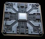
We are advancing several areas:
• Next-generation ML optimization techniques tailored for reconfigurable hardware
• Dynamic model-to-hardware mapping, enabling real-time adaptation to workload changes
• Inference orchestration across heterogeneous infrastructure
• Turnkey deployment platforms that abstract hardware complexity from customers

Our goal is to make high-efficiency AI infrastructure as easy to consume as cloud GPUs—but significantly more efficient.

How do customers normally engage with your company?

Customers potentially can engage with us in three ways:
1. Token-as-a-Service
They can sign up directly to buy tokens from our maintained inference services.
2. Software Subscription
They can buy the hardware and sign up for a monthly/yearly subscription for our inference software
3. Leasing or Purchase
They can order a purchase or lease of a prebuilt rack of our inference infrastructure, fully enabled and ready to generate tokens.

We also partner closely with:
• Cloud providers
• Data center operators
• AI model companies

This allows us to integrate into existing ecosystems while delivering immediate value.

CONTACT ELASTIX.AI

Also Read:

CEO Interview with Jerome Paye of TAU Systems

CEO Interview with Juniyali Nauriyal of Photonect

CEO Interview with Aftkhar Aslam of yieldWerx


Tesla and Samsung Relationship Update

Tesla and Samsung Relationship Update
by Daniel Nenni on 03-15-2026 at 8:00 am

Elon Musk Lip Bu Tan Wafer Deal

The majority of my 40+ year career has been spent managing the relationship between leading-edge semiconductor design and manufacture, working with just about every commercial foundry and top customer in one way or another. It’s my thing—it fascinates me. I’m also a fan of disruption, and the latest disruptions the semiconductor industry has been experiencing are fiercely entertaining.

Which brings us to the Tesla and Samsung relationship update.

In 2025, Tesla and Samsung Electronics announced a deep strategic partnership centered on manufacturing Tesla-designed AI chips used for self-driving vehicles, robotics, and AI infrastructure. The partnership is expected to evolve across multiple hardware generations and already includes one of the largest semiconductor supply agreements ever signed by an automaker. Below is a breakdown of the relationship covering its history, the technical structure of the chips, the manufacturing arrangements, and the strategic reasons behind the partnership.

Key Takeaways

The Tesla–Samsung relationship is a strategic semiconductor alliance built around three core elements:

  • Fabless model: Tesla designs AI chips; Samsung manufactures them.
  • Massive manufacturing deal: A $16.5 billion multiyear contract centered on Tesla’s AI6 chips.
  • AI ecosystem support: Chips produced by Samsung power Tesla’s vehicles, robots, and AI data centers.

The partnership also reflects a broader trend: automakers becoming major semiconductor designers as vehicles increasingly rely on AI and custom compute hardware.

Now let’s look at the relationship from the perspective of a working semiconductor professional—based on observations, experiences, and opinions from inside the industry.

Samsung Foundry Background

Samsung truly became a major force in the foundry business through its early relationship with Apple. Early Apple iProducts were manufactured in partnership with Samsung Foundry.

Samsung Foundry operates as an IDM-style foundry, unlike pure-play foundries such as TSMC or GlobalFoundries. Some of the Samsung content in the iProduct BoMs were from Samsung directly. I am only speaking about the SoC that apple designs and manufactures at a foundry.

Years ago, I served as Director of Foundry Relationships at an IP company, which meant spending a significant amount of time in South Korea, Taiwan, and China. Even though the companies were in the same market segment, doing business with different companies in different countries —especially when compared to working with a U.S.-based foundry was a big challenge.

From my personal experience with Samsung Foundry, I can say I worked with some extremely intelligent engineers developing bleeding-edge technology at a break neck pace. The teams worked incredibly hard and achieved a reasonable amount of market success.

However, there was one consistent challenge: transparency. Samsung Foundry often struggled with openness when issues arose—particularly if those issues might bring embarrassment to the company. Yield challenges are a classic example.

Now mix that culture with Elon Musk’s operating style and you can probably imagine the potential for a highly combustible situation—which is where we are today. Among many colleagues I’ve spoken with, very few believed this partnership had a strong probability of long-term success.

Delays and Industry Reality

Delays with Tesla’s AI6 chip have begun surfacing, and Samsung is—unsurprisingly—being blamed, as every foundry tends to be when a chip misses its schedule. From what I hear, however, the delays are occurring on both sides, so the finger-pointing continues.

This dynamic is nothing new in the semiconductor world. Chip programs are extraordinarily complex, and when schedules slip, the tension between design teams and manufacturing teams can escalate quickly.

As a result, Elon Musk is now talking about Mega Fabs.

The Mega Fab Idea

The “Mega Fab” concept refers to a proposed large-scale semiconductor manufacturing facility dedicated to producing AI chips for Tesla. Musk has suggested that Tesla may eventually build its own advanced chip fabrication plant to support the enormous computing demand required for autonomous driving, robotics, and AI training.

By the way, those of us inside the semiconductor industry would simply call that an IDM mega fab.

And who is the most dominant semiconductor IDM in the history of the industry?

Intel Foundry

If Elon Musk does not work with Lip-Bu Tan and Intel on a project like this, I would give the effort a very small chance of success—absolutely.

Come on, Elon. The Silicon Heartland project in Ohio is ready for mega fabs. America is ready to lead semiconductor manufacturing again.

Let’s get this done before you see something shiny and wander away.

I will write more about a Tesla and Intel relationship next.

Also Read:
Musk says Tesla’s mega AI chip fab project to launch in seven days
Tesla AI6 chip delayed ~6 months as Samsung 2nm production slips

Podcast EP335: The Far Reaching Impact of UCIe with Dr. Debendra Das Sharma

Podcast EP335: The Far Reaching Impact of UCIe with Dr. Debendra Das Sharma
by Daniel Nenni on 03-13-2026 at 10:00 am

Daniel is joined by Dr. Debendra Das Sharma, a Senior Fellow and Chief I/O architect in the Data Platforms and Artificial Intelligence Group at Intel. He is a member of the National Academy of Engineering (NAE), Fellow of IEEE, and Fellow of International Academy of AI Sciences. He is a leading expert on I/O subsystem and interface architecture. He co-invented the chiplet interconnect standard UCIe and is the chair of the UCIe consortium.

Dan and Debendra explore the evolution of the UCIe standard and the work of the UCIe consortium. In a very broad and informative discussion Debendra describes the history and impact of UCIe. He details the specification’s evolution from 1.0 to 3.0, explaining the interoperability each version enabled. He explores how UCIe defines key target metrics for chiplets. He also explains how to achieve a plug and play environment. Dan also explores how UCIe is being deployed in the ecosystem with Debendra as well as how the standard is evolving to meet future needs.

The views, thoughts, and opinions expressed in these podcasts belong solely to the speaker, and not to the speaker’s employer, organization, committee or any other group or individual.


Agentic AI and the Future of Engineering

Agentic AI and the Future of Engineering
by Daniel Nenni on 03-13-2026 at 6:00 am

sassine announces agentic ai hires converge 2026
Sassine Ghazi Synopsys Converge Keynote

Agentic AI emerges in this Synopsys Converge keynote not as a futuristic add-on, but as a practical response to the growing complexity of engineering. In the speaker’s view, the traditional way of designing chips, systems, and intelligent products is no longer sufficient for the era of physical AI. Engineers are now dealing with software-defined systems, advanced silicon, multi-physics constraints, verification challenges, and ever-shorter development cycles. In that environment, agentic AI becomes essential because it helps “re-engineer engineering” itself. Rather than replacing engineers, it is presented as a new layer of intelligence that works alongside them, extending human capability and allowing organizations to handle more ambitious projects with the same or limited engineering resources.

A key tension in the speech is the mixture of excitement and fear surrounding agentic AI. At the user and engineering level, many people worry about how this technology may change their jobs. That concern is understandable, because engineering has long depended on deep human expertise, judgment, and careful iteration. At the same time, the speaker stresses that management and organizational leaders are enthusiastic because they see agentic AI as a productivity multiplier. Companies today are often limited not by ideas, but by the number of engineers available and the amount of time required to turn complex ideas into working products. In that sense, agentic AI is framed less as a threat than as a force multiplier: it can help teams do more, move faster, and explore more design possibilities than would be possible through manual effort alone.

One of the most important parts of the keynote is the framework of autonomy levels from L1 to L5. This structure shows that Synopsys is not treating agentic AI as a vague concept, but as a staged engineering roadmap. At L1, there are co-pilots, which assist users across different parts of the design flow. These tools help engineers interact with software more efficiently and automate limited actions. At L2, the system moves to task agents, where each agent is responsible for a specific task. Here the human engineer still acts as the orchestrator, assigning work to multiple specialized agents. At L3, multi-agent workflows appear, meaning that groups of agents can coordinate with one another to complete broader processes. By L4, the vision becomes much more ambitious: a cognitive layer dynamically orchestrates multiple agents with contextual awareness, allowing the system to reason across tasks instead of simply executing isolated commands. L5 remains an early pathfinding stage, but it represents the long-term vision of far greater autonomy in engineering workflows.

What makes this model especially compelling is that it preserves a central role for the human engineer. The keynote explicitly argues that human engineers become more, not less, important in this environment. Their role shifts upward: instead of performing every task manually, they guide, supervise, and accelerate innovation through collaboration with agent systems. This reflects a broader change in knowledge work. The engineer of the future may spend less time on repetitive implementation details and more time defining intent, setting constraints, evaluating outcomes, and steering exploration. Agentic AI, then, is not just about automation; it is about elevating engineering work to a more strategic and creative level.

The concrete example given in the keynote is the path from specification to RTL. This workflow involves many steps: architectural specification, RTL design, test creation, test planning, formal verification, static verification, coverage analysis, and debugging. Traditionally, these are labor-intensive tasks that often require repeated iterations across different teams and tools. In the agentic model, each of these can be assigned to a dedicated task agent. A higher-level reasoning agent then orchestrates those specialists, ensuring that the outputs align and that the resulting RTL is of sufficient quality for the next design phase. This example shows why agentic AI matters: engineering is not usually blocked by one giant problem, but by the coordination of many interdependent smaller problems. Agentic AI addresses that coordination challenge directly.

Another significant idea in the speech is optionality. Synopsys does not present its agentic platform as a closed black box. Customers may bring their own agents, their own data, and their own infrastructure, whether on-premises or in the cloud. This matters because engineering organizations have different security requirements, workflows, and intellectual property concerns. By allowing customers to plug their own systems into the Synopsys stack, the company acknowledges that the future of agentic AI will likely be open, modular, and multi-model rather than standardized around a single monolithic system.

Bottom line: The keynote connects agentic AI to a broader transformation in science and engineering. In a recorded conversation with Microsoft CEO Satya Nadella, Sassine suggests that the next frontier is not merely natural-language assistance, but systems that can plan, execute, and verify complex engineering tasks using deep domain knowledge. The future will depend on combining general-purpose language models with specialized physics and design models. That vision is especially powerful in fields like EDA, where the tools, feedback loops, and verification frameworks already exist to support highly structured automation. In this sense, agentic AI is not just a productivity tool. It is the beginning of a new engineering paradigm, where human expertise and intelligent agents work together to build the increasingly complex systems of the future.

Also Read:

Efficient Bump and TSV Planning for Multi-Die Chip Designs

Reducing Risk Early: Multi-Die Design Feasibility Exploration

Building the Interconnect Foundation: Bump and TSV Planning for Multi-Die Systems


WEBINAR: Outrunning the Data Wave – Why we need to keep pace with the coming 400% data surge 

WEBINAR: Outrunning the Data Wave – Why we need to keep pace with the coming 400% data surge 
by Daniel Nenni on 03-12-2026 at 10:00 am

A Practical Blueprint for Scaling the Digital Foundation of Silicon Photonics and Co Packaged Optics (1)

The semiconductor manufacturing industry has hit a new era of data intensity. We know that we need to look at alternatives to silicon and that electrical interconnects are unable to keep pace. We know we need to design more chiplets and alter microchip architecture. But how much data are we talking specifically, and how much time do we have to readjust our analytics to keep pace with the tsunami of data that’s around the corner?

The industry’s response has been multifaceted. Advanced semiconductor design strategies, the adoption of chiplets, and the integration of optical I/O and photonics are enabling higher performance, faster AI computation, and increased modularity. These approaches overcome traditional electrical I/O limits and scale functionality across larger, heterogeneous systems. Yet these same innovations generate massive amounts of data, from design simulations to fab telemetry and optical and electrical test results, creating an unprecedented amount of data growth.

REGISTER HERE

Measured per wafer, data volumes have already grown dramatically. Modern fabs with high-frequency sensors, inline inspection, multi-stage electrical testing, and optical characterization tools produce tens of terabytes per day. Compared to 2010, this is roughly 100% growth, highlighting that traditional analytics approaches will increasingly struggle, particularly when integrating diverse datasets across advanced architectures.

Accommodating this growth already requires more precise and detailed data genealogy tracking, now multiply that need by four. Aggregating design and simulation, process development, fab telemetry, metrology and inspection, electrical test, packaging and assembly, and system-level performance shows total data projected to grow 400% or more by 2030. Optical interconnects and photonics add high-resolution measurement streams, further increasing the complexity of correlating test results with process and design variables.

These diverse datasets demand more than storage; they require cross-domain correlation and insight to guide yield, reliability, throughput, and enable quick and precise root cause analytics.

Preparing for the Data Surge: Practical Steps for Engineers

Unified Data Infrastructure — Consolidate heterogeneous datasets across design, fab, metrology, and test environments while normalizing formats and maintaining consistent identifiers across wafers, die, and modules.

Commonality Correlation — Link design simulations, fab telemetry, metrology and inspection data, electrical test results, and optical characterization through shared identifiers to enable correlation across process, design, and performance variables.

Scalable Analytics Workflows — Implement batch or streaming pipelines capable of processing terabyte-scale datasets using distributed frameworks while supporting statistical, spatial, and pattern-based analysis across diverse data formats.

Data Genealogy and Lineage Management — Maintain traceability across design revisions, wafer fabrication, assembly, packaging, and system-level testing to enable faster root-cause analysis and yield optimization.

Operational Insight — Deliver engineering dashboards and automated alerts through tools such as Power BI, enabling faster decision-making across design, manufacturing, and quality teams.

Conclusion

The wave of data approaching semiconductor manufacturing is immense and multifaceted. While per-wafer manufacturing data may double, combined lifecycle datasets, including chiplets, packaging, and optical I/O, are projected to increase fourfold or more by 2030. Preparing now, by building unified, scalable analytics capable of transforming raw data into insight, is essential. Only then can manufacturers harness the benefits of chiplets, advanced design, and photonics without being overwhelmed by the digital tsunami they generate.

Fortunately, tools already exist to help manufacturers harness and organize this rapidly expanding data landscape.

Join our upcoming webinar, Scaling Silicon Photonics and Co-Packaged Optics: A Practical Blueprint for Managing Manufacturing Data, where we will walk through practical approaches for building resilient data infrastructure and analytics workflows for next-generation semiconductor systems.

Also Read:

CEO Interview with Aftkhar Aslam of yieldWerx

Qnity and Silicon Catalyst Light a Path to Success at the Chiplet Summit

Intel Foundry: How They Got Here and Scenarios for Improvement


Ravi Subramanian on Trends that are Shaping AI at Synopsys

Ravi Subramanian on Trends that are Shaping AI at Synopsys
by Daniel Nenni on 03-12-2026 at 8:00 am

Ravi Interview Synopsys Converge

Right before the Synopsys Converge Keynote I caught an interview with Ravi Subramanian, Chief Product Management Officer at Synopsys, which highlights several important trends shaping the future of AI, semiconductor technology, and engineering. His discussion focuses on how the worlds of silicon design and system engineering are converging, driven largely by the rapid growth of AI and the need for more efficient computing infrastructure. The conversation provides insight into the technological, economic, and engineering challenges that will define the next decade of innovation.

Ravi and I are well acquainted. I worked for him at Berkeley DA advising him on foundry strategy and specifically how best to work with TSMC. I held a similar position with Solido Design and was hoping to merge the two companies. Mentor interceded and purchased both Berkley DA and Solido and the rest is as they say history. Interesting enough, the former CEO of Solido Amit Gupta now runs AI Strategy at Siemens EDA. Small world indeed. Two old friends are now competitors, I will comment on that in another article, you will not want to miss this one.

One of the first ideas Ravi discusses is the meaning of the event called “Converge.” This event represents the merging of two traditionally separate engineering communities: silicon engineers and systems engineers. Silicon engineers focus on designing semiconductor chips, while systems engineers design complete products such as cars, medical devices, and industrial machines. In the past, these fields operated somewhat independently. However, modern technologies, especially those powered by AI, require both disciplines to work closely together. For example, autonomous vehicles, robotics, and smart devices rely on specialized chips, complex software, sensors, and physical systems all working together. As a result, the boundaries between hardware and systems engineering are becoming less clear.

Another major theme of the interview is how performance in AI systems is measured. Traditionally, the industry focused on metrics like “tokens per second,” which measures how quickly an AI system can process information. However, Ravi explains that the industry is now paying more attention to efficiency-based metrics such as “tokens per dollar” and “tokens per watt.” These metrics evaluate how much useful AI computation can be performed relative to the cost and the amount of energy consumed. This shift is important because running large AI systems is extremely expensive and energy-intensive. For instance, Ravi mentions that an AI-assisted search query can require four to six times more energy than a traditional search query. As AI becomes more widely used, improving energy efficiency will become one of the most critical challenges in the technology industry.

Ravi also connects AI technology to global economic growth. He explains that the global economy currently produces about $117 trillion in annual output. Of this total, around $41 trillion comes from physical products that require engineering to design and manufacture, while about $60 trillion comes from services. Many economists believe that global GDP could double to around $250 trillion over the next 25 years. According to Ravi, much of this growth will be driven by productivity gains made possible by AI. However, these AI systems rely heavily on advanced semiconductors and computing infrastructure, meaning that the semiconductor industry will play a central role in enabling future economic expansion.

To understand how AI hardware will evolve, Ravi identifies four critical components that determine AI system performance: compute, interconnect, storage, and power. Compute refers to the processors, such as GPUs and specialized AI accelerators, that perform the calculations needed to train and run AI models. Interconnect refers to the technologies that move data between chips and computing nodes. Efficient data movement is crucial because transferring data often consumes more power than performing the computations themselves. Storage, particularly high-bandwidth memory, is another major challenge because modern AI models require enormous amounts of data to operate effectively. Ravi warns that shortages in memory supply could even disrupt certain industries if AI data centers consume most available memory resources. Finally, power consumption is a major constraint because large AI systems require vast amounts of electricity to operate.

The interview also highlights the possibility of significant changes in the semiconductor supply chain. Ravi suggests that the industry is entering the first decade of a major reconstruction as companies adapt their manufacturing processes, design methods, and infrastructure to support the growing AI economy. This transformation will affect everything from chip architecture to memory production and data center design.

Bottom line: Ravi emphasizes that future engineers will need broader knowledge across multiple disciplines. Systems engineers must understand semiconductor technology, while chip designers must understand real-world physics and system behavior. As AI continues to expand into robotics, autonomous systems, and other forms of “physical AI,” the integration of software, hardware, and physical systems will become increasingly important. The convergence of these fields will ultimately define the future of technological innovation.

Also Read:

Efficient Bump and TSV Planning for Multi-Die Chip Designs

Reducing Risk Early: Multi-Die Design Feasibility Exploration

Building the Interconnect Foundation: Bump and TSV Planning for Multi-Die Systems


Axiomise Introduces nocProve to Transform NoC Design Verification

Axiomise Introduces nocProve to Transform NoC Design Verification
by Daniel Nenni on 03-12-2026 at 6:00 am

Axiomise Launches nocProve for NoC Verification

Axiomise has recently launched a new verification tool called nocProve which will transform how Network-on-Chip designs are validated in modern hardware development, absolutely.

The tool is designed to be the first configurable formal verification application specifically created for NoC implementations. It addresses one of the most complex challenges faced by semiconductor engineers and promises to provide a more efficient and thorough approach to ensuring correctness in advanced chip designs.

A Network-on-Chip serves as the communication backbone of complex integrated circuits. These networks route information between processor cores, memory controllers, and specialized accelerators within a chip. NoCs are critical to achieving high bandwidth, low latency, and reliable operation. Every instruction or data transfer in high-performance computing tasks or artificial intelligence workloads relies on these networks functioning correctly. As new custom AI architectures and multi-core processors emerge, designers are creating bespoke NoC configurations to maximize performance and support novel protocols. These custom designs, however, introduce significant verification challenges due to their complexity, multiple clock domains, virtual channels, and advanced routing schemes. Errors such as deadlocks or livelocks can occur in rare circumstances that traditional simulation techniques may not detect.

Formal verification is a method that mathematically proves a design meets its specification under all possible conditions. It is considered the gold standard for ensuring reliability in critical systems. Despite its advantages, formal verification has historically been difficult for NoCs due to the large number of possible states and the nondeterministic behavior of complex designs. Axiomise built nocProve as a configurable application within its existing platform using the company’s proprietary proof engine. This engine is optimized to handle the challenges of formal verification for large, nondeterministic systems. It allows engineers to prove the correctness of their designs exhaustively while reducing the computational burden that often prevents formal methods from completing successfully.

The tool can be adapted to a wide variety of bus protocols, channel types, and routing policies. Engineers submit their designs, usually in hardware description languages such as Verilog or VHDL, along with assertion specifications written in SystemVerilog Assertions. nocProve automatically generates formal proofs to verify that the design conforms to the specifications. This approach allows engineers to catch subtle bugs and corner-case errors that could otherwise go unnoticed until after production. By automating these tasks, nocProve also saves time and reduces the need for labor-intensive manual verification efforts.

The launch of nocProve is significant because traditional verification techniques such as simulation or constrained random testing can only examine a finite set of scenarios. These methods may miss rare but critical faults that could cause functional errors or degrade performance. Formal verification using nocProve provides exhaustive confidence that the design is correct, which is particularly important for high-stakes applications in artificial intelligence accelerators, data centers, and high-performance computing chips. Early detection of potential faults reduces the risk of expensive post-production fixes and silicon respins that can delay product launches.

Axiomise has demonstrated nocProve on real-world NoC designs. The tool was able to verify complex open-source designs with high throughput and multiple simultaneous transactions within a few hours. This speed and reliability showcase the potential for nocProve to be integrated into modern chip development workflows and provide meaningful results early in the verification process. The automation of formal proofs allows design teams to innovate more quickly and with greater confidence, ensuring correctness without sacrificing development time.

Bottom line: nocProve represents a major advance in the formal verification of Network-on-Chip architectures. By automating exhaustive proof generation and efficiently handling complex designs, it addresses one of the semiconductor industry’s most pressing verification challenges. As chips become more customized and performance demands continue to grow, tools like nocProve will be essential for ensuring reliability while accelerating development and reducing the risk of costly errors. Axiomise’s new tool promises to give engineers the confidence to build advanced systems without compromising on correctness or speed.

CONTACT AXIOMISE

Also Read:

Akeana Partners with Axiomise for Formal Verification of Its Super-Scalar RISC-V Cores

IP Surgery and the Redundant Logic Problem

Podcast EP274: How Axiomise Makes Formal Predictable and Normal with Dr. Ashish Darbari


Qnity and Silicon Catalyst Light a Path to Success at the Chiplet Summit

Qnity and Silicon Catalyst Light a Path to Success at the Chiplet Summit
by Mike Gianfagna on 03-11-2026 at 10:00 am

Qnity and Silicon Catalyst Light a Path to Success at the Chiplet Summit

The Chiplet Summit recently concluded. Multi-die heterogeneous design is a hot topic these days and chiplets are a key enabler for this trend. The conference was noticeably larger this year. There were many presentations and exhibits that focused on areas such as how to design chiplets, what standards are important, how to integrate chiplets and what applications show the most promise. All important, exciting and useful topics. There was one session hosted by Silicon Catalyst that stood out for me as different.

Silicon Catalyst is a different kind of organization. One that doesn’t make chips (or chiplets), develop standards or build software design tools. Instead, it has developed a unique, worldwide incubator to bring semiconductor startups from PowerPoint to product. The organization did showcase a number of promising new companies at the show. More on that later. What I want to focus on first is Qnity, a strategic partner of Silicon Catalyst that has substantial size with more than 10,000 employees serving customers in more than 80 countries. This organization is also the last pure-play electronics supplier in the U.S.

The breadth and depth of Qnity create a powerful force for the semiconductor supply chain. Let’s examine how Qnity and Silicon Catalyst light a path to success at the Chiplet Summit

The Silicon Catalyst Footprint

You can learn a lot about Silicon Catalyst and what the organization does on SemiWiki here. Nick Kepler, COO of Silicon Catalyst gave an excellent keynote at the Chiplet Summit that provided some good context as to what the organization does for chiplets and why it’s unique.  Nick explained that Silicon Catalyst is the only accelerator focused on the global semiconductor industry including chips, chiplets, materials, IP and silicon fabrication. Applications include photonics, MEMS, sensors, life science and quantum.

He went on to describe the extensive, worldwide ecosystem that the organization has built. Many organizations have a logo slide. The one from Silicon Catalyst is quite impressive. It is included below.

Silicon Catalyst ecosystem

Qnity and its Unique Impact on the Semiconductor Supply Chain

Chris Gilmore

Chris Gilmore, Advanced Packaging Technology Strategy Leader for Qnity, presented at the Silicon Catalyst session. (The company name is pronounced “Quenity”.) The company was formed when DuPont spun out its electronics business last year, creating a publicly traded (NYSE: “Q”), worldwide force in advanced electronics materials and solutions empowering AI, high performance computing, and advanced connectivity.

Qnity has 39 manufacturing sites and 17 R&D facilities around the world. The majority of its portfolio is tied directly to semiconductors, giving the company a total addressable market exceeding $30 billion. Qnity gains more than 40% of its revenue in interconnect technologies, including metallization chemistry and laminates, alongside thermal materials through subsidiary Laird Performance Materials.  This vast size and technology base is what unlocks the opportunity for a substantial impact on the chiplet market. More on that in a moment.

With a Ph.D. in synthetic organic chemistry and well over a decade of experience in advanced packaging and materials research at Dow Chemical and DuPont, Chris brought substantial knowledge of the current semiconductor supply chain challenges.

He explained that Qnity has two primary areas of focus. In semiconductor technologies, it provides consumable materials and solutions for semiconductor chip fabrication, fab equipment, and advanced display panels. In interconnect solutions, it provides advanced materials, systems and engineering solutions for signal integrity, power management and thermal management to address interconnect challenges. This totals about a $4.75B business for the company. The figure below provides a view of the company’s product mix.

It turns out this broad technology base provides Qnity with a unique perspective to advance chiplet designs. Chris explained that chiplets are a simple concept with a complex execution path. One of the primary drivers of this complexity is the fact that chiplets invert typical supply chain dynamics. He explained that the traditional semiconductor supply chain is characterized by low mix/high volume requirements. Due to the many specialized solutions offered by chiplets, the new chiplet supply chain requires a high mix/low volume dynamic.

He explained that chiplet-based design winners will be chosen by performance against high value challenges in many diverse targeted fields of use. The figure below illustrates the wide impact Qnity has on the entire semiconductor value chain. This is unique to Qnity and is the source of its substantial impact on the chiplet market.

Qnity technology portfolio

Thanks to the incredible breadth of Qnity’s offerings, the company is uniquely positioned to rebalance the semiconductor ecosystem to manage the demands of the new chiplet-based breed of design. Chris described a focus of interdisciplinary investment and innovation to help bring chiplets to fruition with broad and deep collaboration across the supply chain.

If you are contemplating a high-volume chiplet application, Qnity is a company to be aware of, and probably one to work with. You can explore the company’s website here.

To Learn More

Silicon Catalyst has put together a video summary of the Qnity presentation at the Chiplet Summit. You can view it at on the Silicon Catalyst website here. There were many other significant events that were part of the Silicon Catalyst session. Other Silicon Catalyst portfolio companies that presented include:

Athos Silicon delivers safe AI for the physical world with a product called Chiptile, the Athos-designed foundational compute chiplet, and the building block of its Multiple Systems on Chip (mSoC) architecture for safety-critical autonomy across robotics, automotive, and aerospace.

CrossFire Technologies tackles Interconnect challenges with an approach called Wire Abundance. No silicon interposer is required, and the product works with current chiplets, SoCs and memory die, delivering a 10X smaller area.

HEPT Lab provides 3D sensors for harsh environments. The HEPT Lab sensor is based on silicon photonics technology that was developed at CalTech for over 10 years. The goal is to make silicon photonics sensors as ubiquitous as cameras.

Quadric delivers a new approach to scalable AI at the edge with a fully programmable stand-alone processor. The architecture is not an accelerator, but rather a processor that is programmable in C++ and Python.

The Silicon Catalyst session ended with a spirited panel discussion. The participants are shown below. You can see a recording of this panel on on the Silicon Catalyst website here.

And that’s how Qnity and Silicon Catalyst light a path to success at the Chiplet Summit.


Intel Foundry: How They Got Here and Scenarios for Improvement

Intel Foundry: How They Got Here and Scenarios for Improvement
by Mark Webb on 03-11-2026 at 8:00 am

Intel Foundry How They Got Here and Scenarios for Improvement

How do you get a shortage while not growing???

Intel Announced earnings in January. Then David Zinsner presented updates on business this week. David is open when talking and always shares 2-3 things he probably should not share. Often he shares things some of us know, but we cannot present because it is not public. Then he makes it public, Thank you David! Our model for what is happening:

Intel Shortage

Intel is unable to meet demand for processors in Q1 and Q2 2026. Their manufacturing is the constraint. The shortage is not TSMC as Intel specifically mentioned moving wafer starts from CCG to DCAI (TSMC is not used for most DC CPUs). The shortage is not 18A. 18A is not running at full capacity in Fab 52, 18A is not in highest demand (Panther lake is a good CPU but it is expensive). Intel 3 is not what is short. It is still ramping and demand has not increased like expected. What is short is Intel 7/10. Raptor lake/Refresh and older on Client. Sapphire/Emerald Rapids on DC.

These are short despite declining sales and despite Intel losing market share in both Client and Datacenter. Less volume than before and yet somehow it is short.

How did this happen?

Intel had a plan. Develop Intel 3 and Intel 18A. Put products on those nodes and ramp them as fast as possible. Products on both were delayed some but there are two main issues that caused the blowback to older nodes. One: the new products are more expensive and there are limits to the number of customers who want to pay that higher price. Granite Rapids and Sierra Forrest are examples and Panther lake is a new example. Good products but customers like sticking with reorders of older products at a lower price OR are looking at AMD products instead. Two: Both technologies have cost/yield/capex expenses that made it so that it is not financially great to ramp them until they are more mature. Yields, output per tool, wafer cost have slowed the ramp below what was expected in 2024.

The plan a couple years ago was to remove Intel 7 capacity (the node is five years old) and add Intel 3 and 18A. Apparently, they did remove Intel 7 capacity assuming people would jump to new products. Historically, this has always been a problem and Intel was able to deal with it. Tell customers they have to move, Tell them the price of the old product is going up, Tell them they can only have the new product. But Intel is not a monopoly now. People are already leaving Intel for AMD and ARM. Intel cannot force people. Intel customers want Sapphire rapids and Raptor lake. Less expensive, mature and they do what we need. If Intel wont sell it to us, we can look elsewhere. Since Intel is already losing share, this is not good and Intel is not pushing

Result: Intel sales are down, Market share is down, people want the older nodes, Intel cannot force them to new nodes. Intel 7 ships way more wafers than Intel 3 and 18A combined. But Intel doesn’t have enough Intel 7 capacity.

Zinsner alluded to some of these items. The Key points are 18A margins are currently negative, Intel 3 needs to get mature, 18A needs to get mature, and they need people to move to new nodes when they can be ramped cost effectively. Until then they need to add capacity to Intel 7.

Scenarios for Future

Due to DRAM shortages and high prices, The future is murky. We expect 10% less PC sales in 2026. We expect PC OEMS to prioritize lower DRAM PCs. Lunar Lake has no discrete DRAM, many people expect it to sell well. Server CPU units will increase but AMD will take some of that share. The key is to get newer products cost effective, then ramp those fabs, then push customers to those parts using pricing.

Intel is/was planning new CPUs in 2026. Arrow lake refresh. Clearwater forest. Diamond rapids. But the most important part in our opinion is Wildcat Lake. This is a cost reduced Panther lake and our cost model shows it can be a solid replacement for Raptor lake at a competitive price and still make money (Panther lake is in a different market with limited volume). But the key is to get Intel 3 and 18A cost effective so they can push customers to the newest products at a competitive price.

When does all this get better? We expect 18A/Panther lake to get more mature by Jan 2027. It will not be cost effective til then…. And yields are not the only problem. It will then get close to filling Fab 52. We know 90%+ of Nova lake CPUs are on TSMC N2 so that needs to play out as well. Intel 3 will continue to ramp but datacenter products are very slow to ramp so it is not clear when this gets fixed.

In 2028, Intel should have its newest fabs ramped and mature and hopefully CPUs have been pushed to these new nodes. We are not expecting IFS to break even in 2027 without a huge one time writeoff, although Zinsner said it was possible, the numbers don’t seem to add up. After Jan 2028, the goal is to continue to ramp 18A and eventually 14A, convert all product to those nodes and start manufacturing external customer volume. If this happens, IFS could break even by 2030. We can go through the gory details on why this will or wont happen and how to update the projections.

Based on all of this, Intel is revisiting its roadmap. Do they really want a new CPU on Client and Datacenter every year? Should they ramp TSMC parts more? We shall see

We have spreadsheet and models to explain all this and how to see if Intel can change the end of the story.

Mark Webb

www.mkwventures.com

Also Read:

Things From Intel 10K That Make You Go …. Hmmmm

The Next Hurdle AI Systems Must Clear

Why Your LLM-Generated Testbench Compiles But Doesn’t Verify: The Verification Gap Problem