Alchip Technologies has recently reported significant progress in the development of advanced 2nm ASICs, positioning itself as a leader in next-generation semiconductor design for AI and HPC. The announcement highlights Alchip’s efforts to commercialize cutting-edge chip technologies and deliver highly customized silicon solutions for data centers, hyperscalers, and AI infrastructure providers. These developments demonstrate how the company is preparing for the transition to one of the most advanced semiconductor process nodes in the industry.
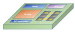
A key milestone in Alchip’s 2nm strategy is the creation of a dedicated 2nm design platform, which enables customers to develop high-performance ASICs using the latest manufacturing technologies. This platform supports advanced packaging and chiplet integration methods such as 2.5D and 3D integrated circuit technologies, allowing designers to combine a 2nm compute die with input/output (I/O) chiplets produced on mature nodes such as 3nm or 5nm. This approach improves yield, reduces cost, and allows developers to integrate complex computing architectures more efficiently.
The transition to 2nm technology represents a major shift in semiconductor architecture. Unlike earlier nodes that relied on FinFET transistor designs, 2nm processes introduce nanosheet or GAA transistors, which provide better electrostatic control and enable higher transistor density. These improvements allow chips to achieve better performance and power efficiency while continuing the scaling trends predicted by Moore’s Law. For AI workloads and large-scale data centers, these advantages are particularly important because they support faster processing speeds and reduced energy consumption.
Alchip has also successfully completed a 2nm test chip tape-out, which is a crucial step in validating the design methodology and manufacturing process. The test chip includes high-speed SRAM blocks and silicon performance monitors that provide real-time insights into chip behavior. These features allow engineers to evaluate PPA characteristics of the new process technology and refine the design flow for future customer products.
Another notable aspect of the test chip is the integration of Alchip’s AP-Link-3D input/output interface, which is designed to support advanced chiplet-based architectures and 3D integration technologies. Chiplet designs divide a large system-on-chip into smaller functional blocks that can be manufactured separately and then connected through high-speed interconnects. This method improves flexibility and scalability, allowing designers to combine different process nodes and specialized components in a single package. The success of the 2nm test chip demonstrates that Alchip’s design tools and intellectual property are ready for these emerging packaging approaches.
Developing chips at the 2nm node also presents significant challenges. The smaller transistor dimensions increase power density and thermal management issues, requiring careful floorplanning, power distribution, and cooling strategies. Alchip’s design methodology addresses these challenges by incorporating thermal-aware design techniques and early optimization of placement and routing. By solving these problems earlier in the design flow, the company aims to reduce development time and improve the likelihood of first-pass silicon success.
The company’s 2nm advancements are closely tied to the broader growth of AI and high-performance computing markets. Many hyperscale data center operators and cloud providers are increasingly turning to custom ASICs rather than off-the-shelf graphics processing units (GPUs) to optimize workloads and reduce operational costs. Alchip specializes in providing these custom silicon solutions, enabling companies to design chips tailored specifically for AI training, inference, networking, and other data-intensive applications. As AI systems continue to grow in complexity, demand for specialized ASIC designs built on advanced nodes such as 2nm is expected to increase significantly.
In addition, Alchip’s work on 2nm technology positions the company for future semiconductor generations. The insights gained from its test chips and design platform will help support the transition toward even more advanced nodes, including potential 1.6nm processes and new transistor architectures. By investing early in design methodologies and packaging technologies, Alchip aims to maintain its leadership in high-performance ASIC development.
Bottom line: Alchip’s reported ASIC-leading 2nm developments highlight a major step forward in semiconductor innovation. Through its new design platform, successful test chip tape-out, and focus on advanced packaging and chiplet integration, the company is preparing customers for the next era of AI-driven computing. These efforts reinforce Alchip’s position as a key player in the global race to deliver faster, more efficient, and highly customized silicon solutions for future technology demands.
Alchip will be at the TSMC 2026 Technical Symposium as will I. You can reach Alchip here. Check out their new website! And of course you can reach me on SemiWiki email if you are a member.
I hope to see you there!
Also Read:
2026 Outlook with Dave Hwang of Alchip
Alchip’s 3DIC Test Chip: A Leap Forward for AI and HPC Innovation