San Diego Arrival
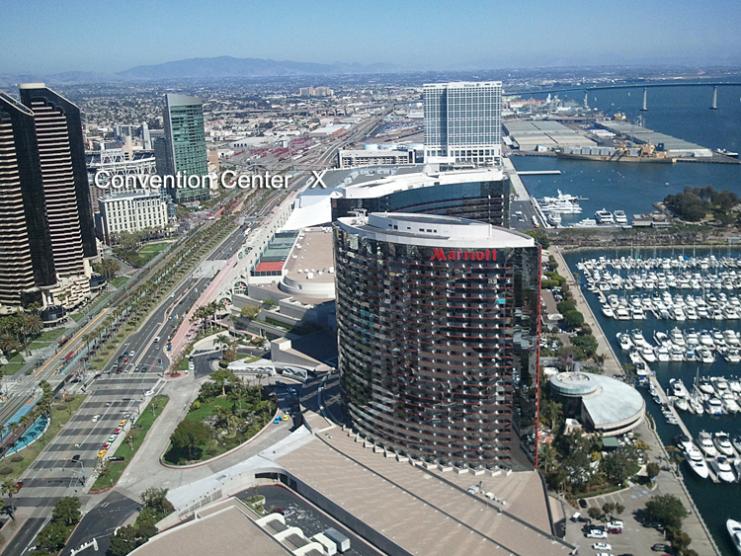
It’s another picture perfect day in San Diego as I arrived and checked into the Hyatt. The view from the 40th floor looked magnificent, with the Convention Center just a few minutes away in the distance:
Registration
Check in at DAC is quite automated and it took only a minute to receive my official badge with an Independent Media sticker.
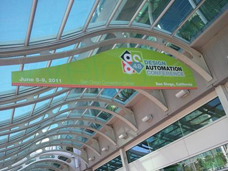
EDAC Party
Tonight is the kick-off event first at 6PM sponsored by EDAC and it’s the annual networking event of the year for us in EDA.
Here I met dozens of former co-workers and EDA clients.
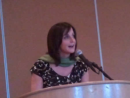
Kathryn Kranen (CEO of Jasper) tried valiantly to address the crowd however the din of networking was just too great. Next year I would try just projecting the key messages on a wall, and let them cycle through instead of live speeches.
Gary Smith
Next up is the 7PM event from Gary Smith EDA. I’m really hoping that these two events are in different rooms so that we may actually get to hear over the roar of networking in the back of the room.
We enjoyed a separate meeting room at Gary Smith’s DAC event on Sunday night. 4G signal coverage was not available with my CLEAR device, so no tweeting this year. Others nearby had zero cell-phone signal as well.
Mary Olsson – 3D packaging. Qualcomm is a big user of TSV and 3D packaging.
Current State of Technology
– TSV: not really cheaper, faster or smaller
– Whatever happened with Multi Chip Modules (MCM)?
– 3 fabs are ready at 200nm now, 300 mm ready in 5 years (too much stress and cracking)
– Today: Mostly memory stacking, wafer stacked SOC, image sensors
3D TSV
– Mostly research and University oriented still
– Bleeding Edge Drivers: Intel, Samsung, Qualcomm, TI, STM, Altera
– Xilinx, Nokia, Nvidia, Broadcom, Cisco
– Tessera, Tezzaron, eSilicon
Standard Drivers : GSA, JEDEC, Si2 Open3D
TSMC Revenue by Technology – 1st quarter numbers, 65% of revenue for 90nm to 40nm nodes, mostly standard packages
– 35% of revenue from above 135nm nodes and larger
Top IDMs and Foundries: Where is their capacity?
– Sweet spot is between 45nm and 60nm
– Intel/Samsung vs everybody else
– Qualcomm driving the bleeding edge of 3D packaging technology
TSMC Foundry Drivers
– 48% communications
– 23% consumer
– 18% industrial
– 11% industrial
PCs – shipped 379M units in 2010
iPad (Tablets) – 136m units in 1Q2011
2015 Time frame – next big push from emerging nations to start consuming personal electronics
What is true 3D/TSV?
– Today we see 2.5 and 3D TMV (stacked die for memory, SOC, SiP, Flip Chip, PoP, Cu pillar bump, many via types
AMKOR photos of molded via, package on package techniques
EDA – Sigrity (Orbit10 Planner), Micro Magic (Max 3D), Apache (RedHawk, Sentinel)
What to look for – OSATs, eSilicon, Tessera, Tezzaron
RF challenges
3D Summary
Read the GSA Guide (Herb Reiter)
Follow the money – OSATs spend money on copper wire bonders, new test equipment
Watch those hiring – Intel, Qualcomm
Gary Smith
EDA 2Q 2011 Forecaast
$4896 2011
$5325 2012
$5671 2013
$5885 2014
$6612 2015
The Semiconductor Infrastructure
– The semi cycle: VC funding, EDA, embedded sw, compute power, process r&d, semi equipment, foundry, packaging
EDA – tools to enable design (at a cost that allows operating at a profit)
Costs – Design companies cost more than EDA tools (embarrassed by low price of EDA tools)
Cost of SOC Design – Keep the cost of a new SOC below $25M will attract VCs again.
– Costs above $50M hurts even IDMs
ITRS Cost Chart for 2010
Is EDA affordable?
Design Teams – 100 to 200 engineers
– For 104 million gates (should be about 30 HW design engineers, costing $18.7m)
– 160 SW engineers cost $56M, total of $75M
Cost Curves for HW Design Teams (Needs to be kept under $25M)
Ideal Number of Blocks: 5
– Most designs have 25 to 35 blocks (more blocks slows design process down)
What is Block Size?
– 100 million gate (90 million gates on platform, 10 million left to design)
– Number of engineers per block 6 engineers
EDA Tools Handle gates?
– 4 million minimum, 20 million needed
At 22nm – need 88m gates capacity
At 16nm – need 177m gates
At 11nm – need 354m gates
R&D Engineers – do you know how design uses the EDA tools?
How to Follow Moores Law?
– Productivity tools, keep close to design engineers
– Get involved in sw productivity
EDA History
– Cadence as technology leader 1990 to 1997
– 2004 to 2007 Fister’s Folly as
– 2003 SNPS is #1 technology after Avant! Acquisition
– 2008 and 2009 SNPS as #1 tech leader
o Mentor and Magma still close in technology
o Who handles 22nm design? Large or small companies?
Summary
The mood at DAC this year is optimistic, there’s talk of hiring and people are eager for the Keynote address on Monday and the flurry of events planned. I’ll be blogging each day as I visit EDA vendors that offer transistor-level tools like: SPICE, DRC, LVS, 3d extraction, Custom IC layout tools, and more. On Tuesday I’ll be at the Panel Session on “3D Extraction: Coming to a Design Near You?“


Silicon Insurance: Why eFPGA is Cheaper Than a Respin — and Why It Matters in the Intel 18A Era