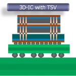
More news from the 3DASIP conference. Chet Palesko of SavanSys Solution had an interesting presentation with the same title as this blog (although this blog draws from several other presentations too). Chet took a look at what aspects of 3D are likely to get cheaper going forward. He took as a starting point that stuff that is not … Read More
Tag: thru silicon via
Hybrid Memory Cube Shipping
Today Micron announced that it is shipping 2GB Hybrid Memory Cube (HMC) samples. The HMC is actually 5 stacked die connected with through-silicon-vias (TSVs). The bottom die is a logic chip and is actually manufactured for Micron in an IBM 32nm process (and doesn’t have any TSVs). The other 4 die are 4Gb DRAM die manufactured… Read More
3D: the Backup Plan
With the uncertainties around timing of 450mm wafers, EUV (whether it works at all and when) and new transistor architectures it is unclear whether Moore’s law as we know it is going to continue, and in particular whether the cost per transistor is going to remain economically attractive especially for consumer markets … Read More
SEMICON Taiwan 3D
SEMICON Taiwan is September 3rd to 6th in TWTC Nangang Exhibition Hall. Just as with Semicon West in July in San Francisco, there is lots going on. But one special focus is 3D IC. There is a 3DIC and substrate pavilion on the exhibit floor and an Advanced Packaging Symposium. Design tools, manufacturing, packaging and testing solutions… Read More
3D Architectures for Semiconductor Integration and Packaging
There is obviously a lot going on in 3D IC these days. And I don’t mean at the micro level of FinFETs which is also a way of going vertical. I mean through-silicon-via (TSV) based approaches for either stacking die or putting them on an interposer. Increasingly the question is no longer if this technology will be viable (there… Read More


