You are currently viewing SemiWiki as a guest which gives you limited access to the site. To view blog comments and experience other SemiWiki features you must be a registered member. Registration is fast, simple, and absolutely free so please,
join our community today!
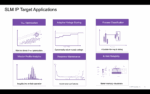
In an era defined by complex chip architectures, ever-shrinking technology nodes and very demanding applications, Silicon Lifecycle Management (SLM) has become a foundational strategy for optimizing performance, reliability, and efficiency across the lifespan of a semiconductor device. Central to effective SLM are Process,… Read More
Power device designers know that when they see a deceptively simple pair of PowerMOS device symbols in the output stage of a power converter circuit schematic, they are actually looking at a massively complex network of silicon and metal interconnect. The corresponding physical devices can have a total device W on the order of … Read More
Often we hear about isolated instances of excellence from various companies in the semiconductor industry which contribute significantly in building the overall ecosystem. While the individual excellence is essential, it’s rather more important how that excellence is utilized in a larger way by the industry to create a ‘value… Read More
If we look back in the last century, performance and area were two main criteria for semiconductor chip design. All design tools and flows were concentrated towards optimizing those two aspects. As a result, density of chips started increasing and power became a critical factor. Now, Power, Performance and Area (PPA) are looked… Read More
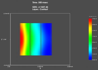
With increasing density and functionality of chips at extremely thin silicon and metal layers, temperature has become critical. The temperature situation can become worse with wireless enabled 24/7 power-on devices. In such a scenario, a device must manage its thermal profile dynamically to keep the temperature within tolerable… Read More