You are currently viewing SemiWiki as a guest which gives you limited access to the site. To view blog comments and experience other SemiWiki features you must be a registered member. Registration is fast, simple, and absolutely free so please,
join our community today!
DesignCon is coming up and the panel discussions look very interesting this year. The one panel session that I recommend most is called, “Analog and Mixed-Signal Design and Verification” which is moderated by Brian Bailey, one of my former Mentor Graphics buddies and fellow Oregonian.… Read More
My wife and I have traveled to Switzerland on vacation and marveled at the natural beauty of the mountains, efficient train system, tasty chocolate, and wonderful foods. I only wished that our American dollar bought more in Swiss currency than it did. Recently I discovered a high-tech IC design company called Microdul that designs… Read More
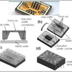
At a webinar today I listened and learned about how a tool called L-Edit can be used to layout MEMS designs plus automate the task to be more productive. I can see how the history of IC layout editing is now being repeated with MEMS because in the earliest IC layout tools we could only do manual entry of polygons, then gradually we got cells… Read More
My automobile has an air bag system that uses a MEMS (Micro Electro Mechanical System) sensor to tell it when to deploy, and I’ve read headlines talking about MEMS over the years so I decided it was about time to learn more by attending a Webinar on Wednesday, December 14th at 8AM Pacific Time.
The EDA company hosting the Webinar… Read More
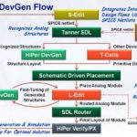
My last IC design at Intel was a Graphics Chip and I developed a layout generator for Programmable Logic Arrays (PLA) that automated the task, so I’ve always been interested in how to make IC layout more push-button and less polygon pushing. Today I watched a video about HiPer DevGen from Tanner EDA and wanted to share what I … Read More
Every analog designer needs a foundry PDK (Process Design Kits) and EDA tools to design, layout and verify their AMS chip or IP. This week I had a chance to conduct an email interview with Taek-Soo Kim, VP of Technical Engineering at Dongbu HiTek in Korea. This specialty foundry supplies analog silicon worldwide.
Interview
Q: Tell… Read More
AnSem has been in the AMS design business since 1998 and uses a variety of commercial EDA tools along with internally developed tools and scripts to automate the process of analog design and technology porting. Their IC designers have completed some 40 AMS projects in diverse areas like:
- RF CMOS
- LNA, VCO, Mixers
- Synthesizers
- Low-IF/Zero-IF
…
Read More
From the President: Another Great YearThanks to innovative, cost-effective technology and excellence in customer support, we’ve just ended fiscal year 2011 (on May 31st) with solid growth. Revenue was up 8%, we added 139 new customers, and we’re continuing to reach out to technology partners for MEMS and for the analog and mixed-signal… Read More
Almost every week I read about a slowing world economy, yet in EDA we have some bright spots to talk about, like Tanner EDA finishing its 24th year with an 8% increase in revenue. More details are in the press release from today.
I spoke with Greg Lebsack, President of Tanner EDA on Monday to ask about how they are growing. Greg has been… Read More
Intro
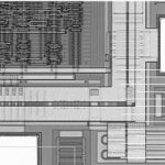
Massimo Sivilotti, Ph.D of Tanner EDA showed me their 3D field solver in the HiPer PX extraction tool at DAC last week.
Notes
Tool Suites – schematics, layout, SPICE simulation, DRC/LVS
– HiPer PX: 3D Field solvero Layers, dielectrics,
o Finite element analysis
o Boundary element methods
o 2D mode for pattern matching… Read More