If we look at the past, most of the EDA tools in the semiconductor design space have originated from a designers’ need to do things faster. Regardless of whether it is design exploration, manual design, simulation, verification, optimization (Power Performance Area – PPA) and many other steps in the overall design flow.… Read More

Tag: spyglass power
A Power Optimization Flow at the RTL Design Stage
SoC designers can code RTL, run logic synthesis, perform place and route, extract the interconnect, then simulate to measure power values. Though this approach is very accurate, it’s also very late in the implementation flow to start thinking about how to actually optimize a design for the lowest power while meeting all… Read More
Smart Clock Gating for Meaningful Power Saving
Since power has acquired a prime spot in SoCs catering to smart electronics performing multiple jobs at highest speed; the semiconductor design community is hard pressed to find various avenues to reduce power consumption without affecting functionality and performance. And most of the chips are driven by multiple clocks that… Read More
RTL Power Analysis and Verification
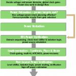
“Power is the new timing” has almost become a cliché. There are a number of reasons for this, not least that increasingly it is power rather than anything else that caps the performance that a given system can deliver. Power is obviously very important in portable applications such as smartphones because it shows through directly… Read More