You are currently viewing SemiWiki as a guest which gives you limited access to the site. To view blog comments and experience other SemiWiki features you must be a registered member. Registration is fast, simple, and absolutely free so please,
join our community today!
Formal Going Mainstreamby Paul McLellan on 07-10-2012 at 7:29 pmCategories: EDA
In Mike Muller’s keynote at DAC he wanted to make formal approaches an integral part of writing RTL. After all, formal captures design intent and then, at least much of the time, can verify whether the RTL written actually matches that intent. Today, formal is not used that way and is typically something served “on the side” by specialist… Read More
One of the truisms of today’s disaggregated semiconductor design and manufacturing model is counter-intuitive to the do-it-yourself focus that is at the heart of every engineer. And yet, time and time again, success rewards those who understand that with today’s ever increasing complexity, it is difficult, if… Read More
Next week it is Semicon West in the Moscone Center from Tuesday to Thursday, July 10-12th. Cadence will be on a panel session during a session entitled The 2.5D and 3D packaging landscape for 2015 and beyond. This starts with 3 short keynotes:
- 1.10pm to 1.25pm: Dr John Xie of Altera on Interposer integration through chip on wafer on
…
Read More
Minitel Shuts Downby Paul McLellan on 07-05-2012 at 5:02 pmCategories: General
When I first came to the US, one project that we had going on at VLSI Technology was an ASIC design being done by a French company called Telic. The chip would go into something called “Minitel” which the France Telecom (actually still the PTT since post and telecomunications had not yet been separated) planned to supply… Read More
In my circuit design past I did DRAM work at Intel, so I was interested in learning more about Novocell Semiconductor and their design of One Time Programmable (OTP) IP. Walter Novosell is the President/CTO of Novocell and talked with me by phone on Thursday.… Read More
For those of you who didn’t get to DAC you can catch up on low power issues with Apache’s series of low-power webinars taking place late in July. All webinars are at 11am Pacific Time. Full details and registration on the Apache website here.… Read More
Crushed Blackberryby Paul McLellan on 07-02-2012 at 12:00 amCategories: General
I wasn’t going to write about the cell phone business again for some time. After all, this is a site about semiconductor and EDA primarily. But the cell-phone business in all its facets is a huge semiconductor consumer and continues to grow fast (despite my morbid focus on those companies that do anything but).
But Research… Read More
Everyone knows Moore’s Law: the number of transistors on a chip doubles every couple of years. We can take the process roadmap for Intel, TSMC or GF and pretty much see what the densities we will get will be when 20/22nm, 14nm and 10nm arrive. Yes the numbers are on track.
But I have always pointed out that this is not what drives… Read More
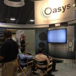
Chip Synthesis at DACby Paul McLellan on 06-27-2012 at 8:30 pmCategories: EDA
I visited Oasys Design Systems and talked to Craig Robbins, their VP sales. For the first time this year, Oasys has a theater presentations and demos of RealTime Designer which are open to anyone attending the show. In previous years, they have had suite demos for appropriately qualified potential customers but outside they have… Read More
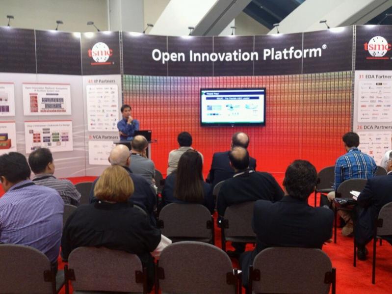
Lorentz Solution presented at TSMC’s DAC 2012 Open Innovation Platform Theater. The presenter was Lorentz Sales Director, Tom Simon. He presented what Lorentz calls its Electromagnetic Design and Analysis Platform. One of the main points of the talk was the cooperative work that Lorentz does with TSMC.
TSMC and Lorentz work … Read More