You are currently viewing SemiWiki as a guest which gives you limited access to the site. To view blog comments and experience other SemiWiki features you must be a registered member. Registration is fast, simple, and absolutely free so please,
join our community today!
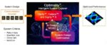
Most IC and system engineers follow a familiar process when designing a new product: create a model, use parameters for the model, simulate the model, observe the results, compare results versus requirements, change the parameters or model and repeat until satisfied or it’s time to tape out. On the EDA side, most tools perform… Read More
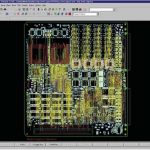
After teams sweat the details of SoC and industrial design, they turn to printed circuit board designers for magic. Here are a pile of chips and passives, and a schematic for interconnecting them. This is how much physical space the board can occupy. Connectors have to be here, and here, and mounting holes there, and there. There … Read More
In the 1990’s there was a push to build EDA frameworks, however they all failed because no user wanted to be locked into one EDA vendor tool flow. Fast forward to 2014 and there’s an emerging trend to use web-based EDA tools as a framework, instead of downloading and installing software to your desktop or device. I just… Read More
Archaic tech metaphors abound, stuck in the psyche of users everywhere. We still “dial” numbers, long after the benefit of a short pull area code disappeared. (Humans could dial 1, 2, or 3 a lot faster on a rotary phone, and there were fewer dialpulses for central office switches to decode – thus big cities with more phone traffic like… Read More