You are currently viewing SemiWiki as a guest which gives you limited access to the site. To view blog comments and experience other SemiWiki features you must be a registered member. Registration is fast, simple, and absolutely free so please,
join our community today!
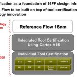
Today TSMC announced three reference flows that they have been working on along with various EDA vendors (and ARM and perhaps other IP suppliers). The three new flows are:
- 16FinFET Digital Reference Flow. Obviously this has full support for non-planar FinFET transistors including extraction, quantized pitch placement, low-vdd
…
Read More
At TSMC’s OIP on October 1st, Mentor Graphics have 5 different presentations. Collect the whole set!
11am, EDA track. Design Reliability with Calibre Smartfill and PERC. Muni Mohan of Broadcom and Jeff Wilson of Mentor. New methodologies were invented for 28nm for smart fill meeting DFM requirements (and at 20nm me may … Read More
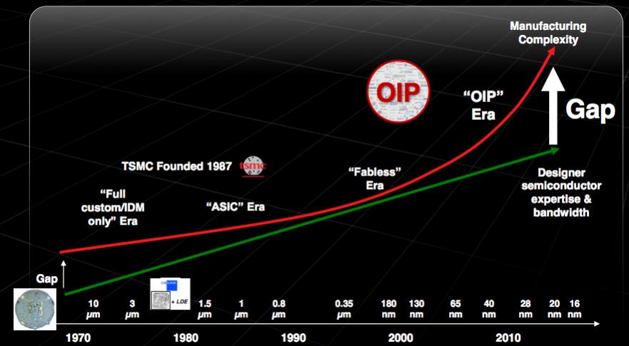
The history of TSMC and its Open Innovation Platform (OIP) is, like almost everything in semiconductors, driven by the economics of semiconductor manufacturing. Of course ICs started 50 years ago at Fairchild (very close to where Google is headquartered today, these things go in circles). The planarization approach, whereby… Read More
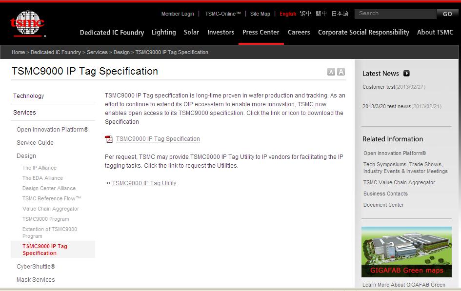
We have seen last week in a first post how crucial was the IP qualification process (TSMC 9000) to increase the probability of successfully Tape Out a chip. Being able to discriminate between dangerous and safe IP is the first step of TSMC 9000 Quality process, IP tagging is the complementary step, almost as essential as the first … Read More
Fabless to OIPby Paul McLellan on 04-10-2013 at 7:22 pmCategories: Uncategorized
Suk Lee drew the short straw at the TSMC Symposium yesterday, with the 5pm slot. Not only late in the day but between all the attendees and free beer. The morning sessions had been standing room only, with several hundred standees (as they call them on muni around here, but isn’t a standee really someone being stood on?). But … Read More


