You are currently viewing SemiWiki as a guest which gives you limited access to the site. To view blog comments and experience other SemiWiki features you must be a registered member. Registration is fast, simple, and absolutely free so please,
join our community today!
After 8 SemiWiki years, 4,386 published blogs, and more than 25 million blog views, I can tell you that IP is the most read semiconductor topic, absolutely, and that trend continues. Another correlating trend (from IP Nest) is the semiconductor IP revenue increase in relation to the semiconductor market (minus memory) which more… Read More
Once upon a time, RAM technology was the driver of the semiconductor process. DRAM products were the first to be designed on a newest technology node and DRAM was used as a process driver. It was 30 years ago and the most aggressive process nodes were ranging between 1um and 1.5 um (1 500 nm!). Then in the 1990 the Synchronous Dynamic … Read More
While looking for information on a Xilinx Spartan 6 Project with DDR memory I came across a new type of DRAM called the Hybrid Memory Cube (HMC). The technology made me want to take a closer look:
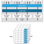
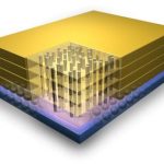
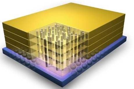
The Hybrid Memory Cube is like a stack of DDR chips stacked die on die using through silicon vias to interconnect the dies the bottom die in not… Read More
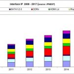
The reader will find many updates in the “Interface IP Survey” from IPNEST, released in October 2013. Good question, as the IP market is a very fast moving one and the protocol based Interface IP, is moving even faster… exhibiting 20% growth rate in 2012, expected to grow with 10% CAGR between 2012 and 2017 to reach $700M. … Read More
Today Micron announced that it is shipping 2GB Hybrid Memory Cube (HMC) samples. The HMC is actually 5 stacked die connected with through-silicon-vias (TSVs). The bottom die is a logic chip and is actually manufactured for Micron in an IBM 32nm process (and doesn’t have any TSVs). The other 4 die are 4Gb DRAM die manufactured… Read More
That’s too bad, as you have missed latest news about the Hybrid Memory Cube (presentation by Micron), Wide I/O 2 standard, as well as other standards like LPDDR4, eMMC 5.0, and LRDIMM,the good news is that you may find all these presentations on MemCon proceedings web site.
I first had a look at Richard Goering excellent blog: wideI/O… Read More
Perhaps no semiconductor company took it on the chin harder the last half of 2011 than Micron. And yet, perhaps no company was racing as hard as Micron to make a radical changeover. Micron is considered a bell weather on the overall health of the semiconductor industry given that DRAM, NAND and NOR Flash are used in some combination… Read More