You are currently viewing SemiWiki as a guest which gives you limited access to the site. To view blog comments and experience other SemiWiki features you must be a registered member. Registration is fast, simple, and absolutely free so please,
join our community today!
Intel Foundry and ASML say high-numerical-aperture extreme-ultraviolet lithography has crossed an important boundary: it is no longer only a development tool, but a production technology. At the SPIE Photomask Technology and Extreme Ultraviolet Lithography conference, the companies reported that Intel has processed … Read More
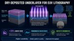
Extreme-ultraviolet lithography is essential for manufacturing advanced semiconductor devices, but its continued scaling presents a difficult materials problem. Photoresists must simultaneously provide high resolution, low exposure dose, limited line-edge or linewidth roughness, and extremely low defectivity. … Read More
Extreme ultraviolet (EUV) lithography systems are the most advanced lithography systems in use today. This article is a basic primer on this important yet complex technology.
The Goal: A Smaller Wavelength
The introduction of 13.5 nm wavelength continues a trend the semiconductor industry had been following a wavelength reduction… Read More