You are currently viewing SemiWiki as a guest which gives you limited access to the site. To view blog comments and experience other SemiWiki features you must be a registered member. Registration is fast, simple, and absolutely free so please,
join our community today!
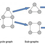
I think by now a lot has been said about the necessity of multi-patterning at advanced technology nodes with extremely low feature size such as 20nm, because lithography using 193nm wavelength of light makes printing and manufacturing of semiconductor design very difficult. The multi-patterning is a novel semiconductor manufacturing… Read More
In this age of SoCs with hundreds of IPs from different sources integrated together and working at high operating frequencies, FPGA designers are hard pressed keeping up the chip reliability from issues arising out of excessive static & dynamic IR drop, power & ground noise, electro migration and so on. While the IPs are… Read More
As chips have become larger, one of the more challenging steps is full-chip signoff. Lots of other steps in the design process can work on just a part of the problem, but by definition full-chip signoff has to work on the full chip. But it is not just that chips have got larger, the number of corners that need to be validated has also exploded.… Read More