You are currently viewing SemiWiki as a guest which gives you limited access to the site. To view blog comments and experience other SemiWiki features you must be a registered member. Registration is fast, simple, and absolutely free so please,
join our community today!
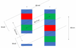
For the so-called “2nm” node or beyond, the minimum metal pitch is expected to be 20 nm or even less, while at the same time, contacted gate pitch is being pushed to 40 nm [1]. Therefore, we expect via connections that can possibly be as narrow as 10 nm (Figure 1)! For this reason, it is natural to expect High-NA EUV lithography as the go-to
…
Read More
While stochastic defects link yield with the practical resolution of EUV lithography resulting from its quantum nature [1], very low yields of EUV processes are more readily linked to the use of EUV masks without pellicles. Pellicles are thin film membrane covers on masks (regardless of wavelength: EUV and DUV and i-line) used… Read More
The relentless miniaturization of semiconductor devices has always relied on achieving ever-smaller features on silicon wafers. However, as the industry enters the realm of extreme ultraviolet (EUV) lithography, it faces a critical barrier: stochastics, or the inherent randomness in patterning at atomic scales. This phenomenon… Read More
In High-NA EUV lithography systems, the numerical aperture (NA) is expanded from 0.33 to 0.55. This change has been marketed as allowing multi-patterning on the 0.33 NA EUV systems to be avoided. Only very recently have specific examples of this been provided [1]. In fact, it can be shown that double patterning has been implemented… Read More
A comprehensive update to the EUV stochastic image model
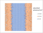
In extreme ultraviolet (EUV) lithography, photoelectron/secondary electron blur and secondary electron yield are known to drive stochastic fluctuations in the resist [1-3], leading to the formation of random defects and the degradation of pattern fidelity at advanced
…
Read More
Peak probability at zero distance actually makes no sense
In lithography, it is often stated that the best resolution that can be achieved depends on wavelength and numerical aperture (NA), but this actually only applies to the so-called “aerial” image. When the image is actually formed in the resist layer, it also depends on an… Read More
Whether EUV or DUV doesn’t matter at 20 nm pitch
The International Roadmap for Devices and Systems, 2022 Edition, indicates that the “2nm” node due in 2025 (this year) has a minimum (metal) half-pitch of 10 nm [1]. This is, in fact, less than the resolution of a current state-of-the-art EUV system, with a numerical aperture… Read More
Previously, I had indicated how detrimental stochastic effects at pitches below 50 nm should lead to reconsidering the practical resolution limit for EUV lithography [1]. This is no exaggeration, as stochastic effects have been observed for 24 nm half-pitch several years ago [2,3]. This then leads to the question of whether … Read More
– Lam reports another flat quarter & guide- No recovery in sight yet
– Seems like no expectation of recovery until 2025- Mixed results
– DRAM good- NAND weak- Foundry/Logic mixed-Mature weakening
– Clearly disappointing to investors & stock hoping for a chip recovery
Another Flat Quarter &
…
Read More
On Friday April 12th Intel held a press briefing on their adoption of High NA EUV with Intel fellow and director of lithography Mark Phillips.
In 1976 Intel built Fab 4 in Oregon, the first Intel fab outside of California. With the introduction of 300mm Oregon became the only development site for Intel with large manufacturing, development,… Read More