You are currently viewing SemiWiki as a guest which gives you limited access to the site. To view blog comments and experience other SemiWiki features you must be a registered member. Registration is fast, simple, and absolutely free so please,
join our community today!
Earlier this week I went to the Synopsys Interoperability Forum. The big news of the day turned out to be Synopsys wanting to be more than interoperable with Magma, but that only got announced after we’d all gone away.
Philippe Margashack of ST opened, reviewing his slides from a presentation at the same forum from 10 years … Read More
David Liu receeived the Kaufman award for 2001 at the Kaufman award dinner a few weeks ago.
Or to be more formal about it:Dr. C. L. David Liu, the William Mong honorary chair professor of Computer Science and former president of the National Tsing Hua University in Hsinchu, Taiwan, will be presented with this year’s Phil Kaufman Award… Read More
The Nintendo Wii is one of the most successful gaming platforms with the most diverse set of games — from fun games that can be enjoyed by the whole family to fitness programs that can be used by adults. They beat the dominant Sony Playstation and the Microsoft Xbox by thinking outside the box and creating a platform that was really… Read More
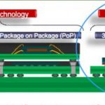
3D-IC design has become a popular discussion topic in the past few years because of the integration benefits and potential cost savings, so I wanted to learn more about how the DRC and LVS flows were being adapted. My first stop was the Global Semiconductor Alliance web site where I found a presentation about how DRC and LVS flows were… Read More
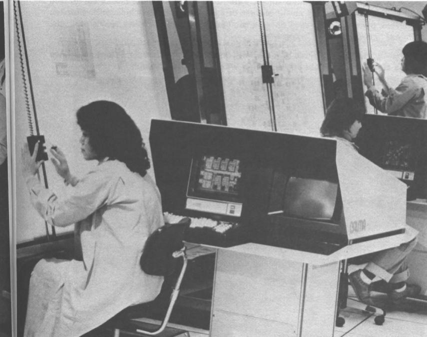
I just put up a blog about the EDA interoperability forum, much of which is focused on standards. Which reminded me just how long-lived some standards turn out to be.
Back in the late 1970s Calma shipped workstations (actually re-badged Data General minicomputers) with a graphic display. That was how layout was done. It’s… Read More
The 24th Interoperability Forum is coming up at the end of the month on November 30th to be held at the Synopsys compus in Mountain View. It lasts from 9am until lunch (and yes, Virginia, there is such a thing as a free lunch). I think it looks like a very interesting way to spend a morning.
Here are the speakers and what they are speaking… Read More
Managing Test Power for ICsby Beth Martin on 11-07-2011 at 12:17 pmCategories: EDA, Siemens EDA
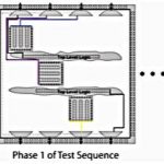
The goal for automatic test pattern generation (ATPG) is to achieve maximum coverage with the fewest test patterns. This conflicts with the goals of managing power because during test, the IC is often operated beyond its normal functional modes to get the highest quality test results. When switching activity exceeds a device’s… Read More
Hello Daniel,
I am very interested on the articles on the PVT simulation, I have worked in that area in the past when I worked in process technology development and spice modeling and I also started a company called Device modeling technology (DMT) which built a Spice model library of discrete components, such as Bipolar/MOS /POWER… Read More
Wow! We always hear semiconductor companies complain about the lack of innovation amongst the EDA leaders. Placing high on the Deloitte 500 list shows that innovation is alive and well in EDA and it IS possible to have a meaningful impact regardless of your overall size. It is worth noting that there are very few EDA companies that… Read More