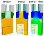
Semiconductor fabs aim to have high yields and provide processes that attract design firms and win new design starts, but how does a fab deliver their process nodes in a timely manner without having to run lots of expensive silicon through the line? This is where simulation and TCAD tools come into play, and to learn more about this… Read More
Tag: cmos
IEDM 2025 – TSMC 2nm Process Disclosure – How Does it Measure Up?
Initial thoughts
At IEDM held in December 2024, TSMC presented: “2nm Platform Technology featuring Energy-efficient Nanosheet Transistors and Interconnects co-optimized with 3DIC for AI, HPC and Mobile SoC Applications,” the authors are:
Geoffrey Yeap, S.S. Lin, H.L. Shang, H.C. Lin, Y.C. Peng, M. Wang, PW Wang, CP Lin, KF… Read More
CEO Interview: Dr Josep Montanyà of Nanusens
Dr. Josep Montanyà Chief Executive Officer – UK/Spain Co-founder leading the company, with +18 years of experience in MEMS, patents and the semiconductor industry. Founded Baolab Microsystems prior to Nanusens.
Tell us a little bit about your company?
We have a patented technology that allows us to build chips with nano-mechanisms… Read More
IEDM 2023 is Coming in December
Anyone who has read my previous IEDM articles will know I view it as one of the best conferences on semiconductor process technology. From the tutorials, short courses and the conference papers there are so many great opportunities to keep up to date on the latest developments. The following are the conference organizers’ announcements… Read More
IEDM 2022 is shaping up
IEDM is one of the premiere conferences for the latest information on leading edge semiconductor technology. The 68th annual International Electron Devices Meeting will be held December 3rd through 7th at the San Francisco Hilton.
The paper submission deadline is July 14, 2022, and the late-news deadline is August 22, 2022. … Read More
Intel Evolution of Transistor Innovation
Intel recently released an exceptional video providing an insightful chronology of MOS transistor technology. Evolution of Transistor Innovation is a five-minute audiovisual adventure, spanning 50 years of Moore’s Law. Some of the highlights are summarized below, with a few screen shot captures – the full video is definitely… Read More
CMOS Forever?
Today, the CMOS chip manufacturing is the pinnacle of the human technology defining economy, society and perhaps us as modern humans. This was highlighted by the recent chip shortage, followed by the ‘shocking’ realization that more than 80% of all chips are manufactured in the Far East.
Important decisions need to be taken by … Read More
Where is the Monument of the Silicon Glen?
In 1991, I arrived in Glasgow to become a lecturer in Glasgow University, attracted by the Silicon Glen – the heart of semiconductor manufacturing in Europe. Here are few facts:
- The larges semiconductor plant in Europe at that time was the NEC DRAM manufacturing site in Livingstone. When I visited the plant, I was mesmerized
This is a Different GLOBALFOUNDRIES!
Having followed GF since its inception, I agree with CTO Gary Patton, what we are seeing today truly is a different GLOBALFOUNDRIES! Our first GF blog was published on 9/13/2009 and we have done a total of 173 GF related blogs that have collected more than 1.5M views thus far. 72 of those blogs were written by me so I have followed this… Read More
Fusing CMOS IC and MEMS Design for IoT Edge Devices
In my 34 years in IC and EDA, it never ceases to amaze me as to how ingenious designers can be with what is given them. Mentor, a Siemens business, has released a wonderful white paper that is proof of this yet again. The white paper steps through how one of their customers, MEMSIC, used the Tanner tool suite to develop a combination CMOS… Read More