As you may know I enjoy poking fun at the current state of semiconductor design and manufacture media; sloppy reporting, editors with little or no actual semiconductor experience taking corporate marketing spins on news/events and passing it along as fact.
Last week it was the EETimes parroting the Samsung foundry business press. A nice thing about being a blogger and owning your own domain is that you get to see (Google Analytics) where the views come from and which links they click on etc…. It’s like spying on your siblings, not that I ever did that. Lets just say that last week South Korea discovered my blog.

This time it is the ElectronicsWeakly top viewed article TSMC Loses 40K Wafers In Quake by one of my fellow bloggers David Manners. There was a lot of press on this topic last week but David is the only one to put a number (40,000 wafers, which is significant) on the loss, and he led with it in an article versus his blog (insert sinister music here). The question is: Where did David get a 40,000 wafer loss number? Certainly not from the official TSMC press brief:
TSMC Reports Impact From March 4 Earthquake Initial Estimate of 1.5 Days Wafer Movement Loss
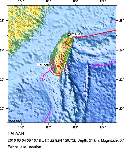
Issued by: TSMC Issued on: 2010/03/04 Hsinchu, Taiwan, R.O.C. – March 4, 2010 – TSMC (TWSE: 2330, NYSE: TSM) today announced that an earthquake of magnitude 6.4 on the Richter scale occurred in south Taiwan at 8:18 am Taiwan local time on March 4. The earthquake registered on instruments at TSMC’sTainansite at magnitude 5, and was measured at TSMC’s Hsinchu site at magnitude 2.
Current assessments reports show that the earthquake had minimal impact on Hsinchu fabs. WhileTainan fabs suffered greater impact, they have gradually begun to resume production. Our initial estimate is that the earthquake caused the equivalent of 1.5 days loss of wafer movement for the company in total.

Luckily one of my siblings, that I absolutely did not spy on when I was a kid, spent his career with semiconductor equipment manufacturers and knows of such things. He says that determining actual wafer or die loss in this context is next to impossibleand here is why:
There are 300+ steps in wafer production so the impact is spread over a long wafer movement process.Average wafer movement loss is calculated as: Each Fab’s Equipment Production Time Loss (including equipment check and recalibration) + Each Fab’s Wafer Scrap (wafers removed from the movement process and not returned) / by over all wafer movement for the company (TSMC). Average wafer movement loss is expressed in “days loss of wafer movement”, which is an averaged manufacturing index, not an actual wafer scrap or revenue loss number. Bottom line, you can’t determine actual “lost wafers” from “loss of wafer movement”.

It looks like David took TSMC’s 2009 capacity of 9,995,000 8-in wafers (the 8-in. equivalent number is used to normalize 6,8, and 12-in. wafer production) and divided it out using 1.5 days of “wafer movement loss” as “lost wafer production”. My emails to David on the subject were not returned. Even funnier, I was in Taiwan that week. Funny because my Taiwan friends accuse me of bringing earthquakes with me from California. As I blogged last year, I was in Taiwan for both the July 2009 and the September 1999 earthquakes, also typhoons and an airplane crash. Pure coincidence I assure you.
Share this post via:


