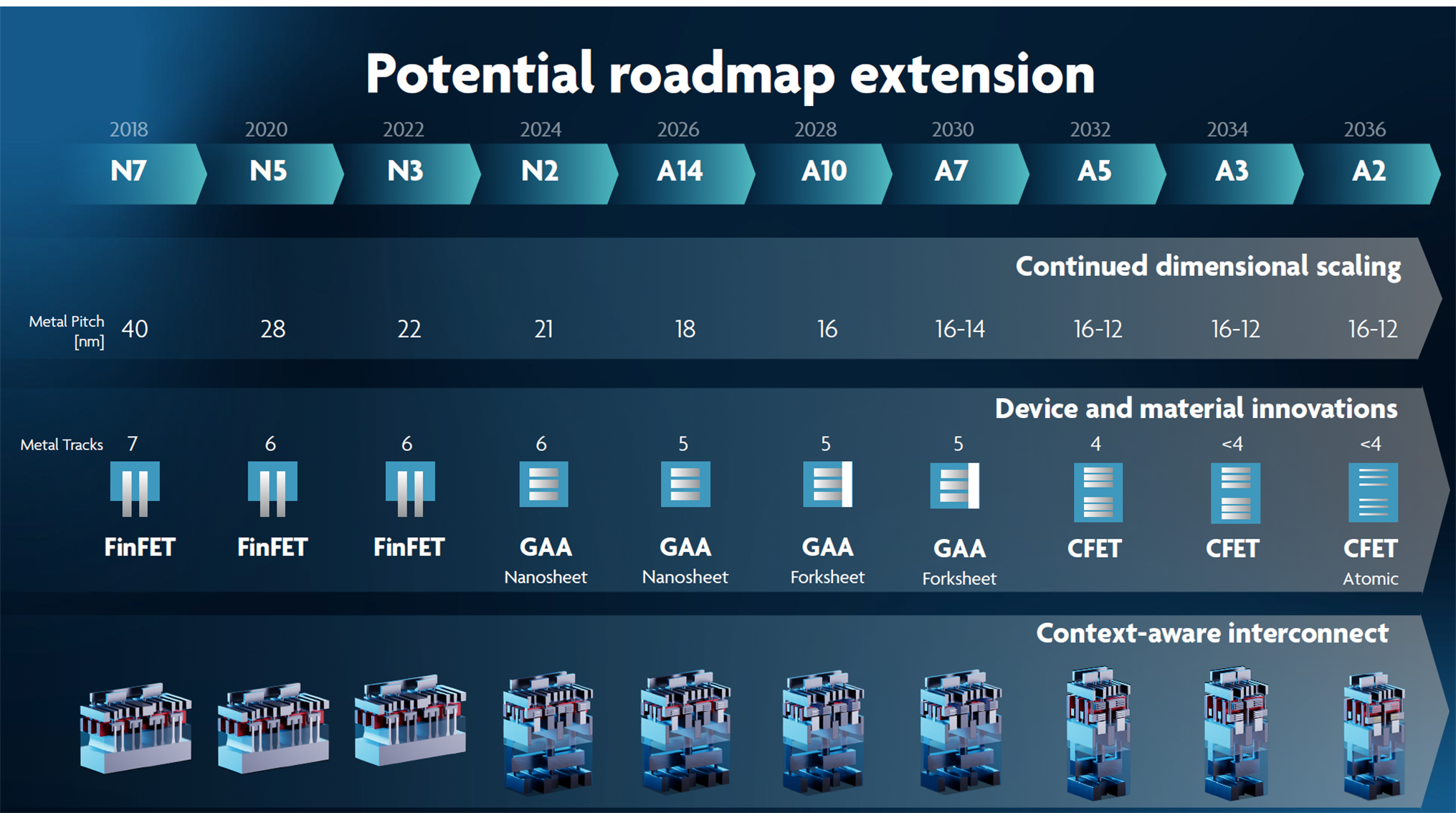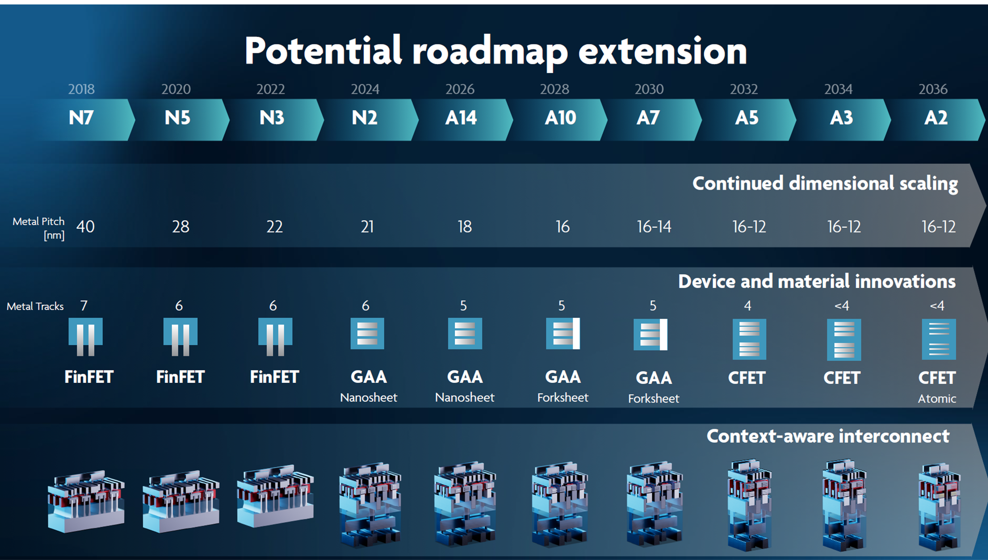
NanoIC has announced a major expansion of its process design kit portfolio with the introduction of its first A14 logic and embedded eDRAM memory PDK. This milestone reflects the company’s growing role in enabling advanced semiconductor design at cutting-edge technology nodes and addresses increasing industry demand for highly integrated, power-efficient system-on-chip (SoC) solutions.
As semiconductor processes continue to scale, the availability of robust and well-validated PDKs has become a critical success factor for chip designers. A PDK serves as the essential interface between a foundry’s manufacturing process and EDA tools, providing accurate models, design rules, device libraries, and verification decks. By extending its portfolio to include A14-class technology, NanoIC is positioning itself to support next-generation designs for applications such as AI, HPC, mobile processors, and advanced networking.
The newly released A14 logic PDK is designed to address the challenges associated with extreme scaling, including tighter design rules, increased variability, and complex power-performance trade-offs. NanoIC’s solution offers comprehensive transistor models, standard cell support, and reliability data that allow designers to confidently optimize performance, power consumption, and silicon area. This is especially important at advanced nodes, where even small inaccuracies in modeling can lead to costly redesigns or yield issues.
What sets this announcement apart is the inclusion of an eDRAM memory PDK alongside the logic offering. Embedded DRAM has re-emerged as an attractive memory option for advanced SoCs due to its higher density compared to SRAM and lower latency compared to off-chip DRAM. Integrating eDRAM directly on logic chips enables designers to build memory-rich architectures that improve bandwidth and energy efficiency, key requirements for data-intensive workloads such as AI inference and edge computing.
NanoIC’s A14 eDRAM PDK provides designers with the tools needed to seamlessly integrate memory blocks into complex SoC designs. The PDK includes memory cell libraries, timing and power models, and process-aware design rules that ensure manufacturability and reliability. By aligning the eDRAM PDK closely with the A14 logic process, NanoIC enables tighter co-optimization between logic and memory, reducing design complexity and accelerating time-to-market.
Another important aspect of the new PDKs is their compatibility with leading EDA platforms. NanoIC has emphasized interoperability and early design enablement, allowing customers to begin architectural exploration and IP development well before volume manufacturing. This early access is increasingly valuable as design cycles lengthen and the cost of advanced-node development continues to rise.
From a broader industry perspective, NanoIC’s move highlights a growing trend toward specialized and differentiated PDK offerings. As advanced nodes become more complex, chipmakers are seeking partners that can provide deep process expertise and tailored design enablement rather than one-size-fits-all solutions. By delivering both logic and eDRAM PDKs at the A14 level, NanoIC demonstrates its ability to support heterogeneous integration and memory-centric architectures that define modern semiconductor innovation.
Bottom line: NanoIC’s extension of its PDK portfolio with its first A14 logic and eDRAM memory PDK represents a significant step forward for the company and its customers. The new offerings address the technical demands of advanced semiconductor design while enabling higher performance, greater integration, and improved power efficiency. As the industry continues to push the limits of scaling and system complexity, comprehensive PDK solutions like NanoIC’s will play a crucial role in turning ambitious chip concepts into manufacturable reality.
Also Read:
TSMC’s 2026 AZ Exclusive Experience Day: Bridging Careers and Semiconductor Innovation
TSMC’s CoWoS® Sustainability Drive: Turning Waste into Wealth
Share this post via:


Comments
There are no comments yet.
You must register or log in to view/post comments.