

As semiconductor scaling slowed and system performance became increasingly constrained by data movement rather than raw compute, advanced packaging emerged as a decisive lever. Among these technologies, TSMC’s CoWoS (Chip-on-Wafer-on-Substrate) represents a turning point in how high-performance systems are architected, manufactured, and scaled. Its evolution mirrors the industry’s shift from transistor-centric progress to system-level optimization.
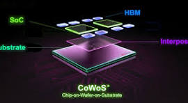
At its core, CoWoS is a 2.5D integration technology. Logic dies and memory stacks are placed side by side on a silicon interposer, which is then mounted onto an organic substrate. The silicon interposer enables wiring densities far beyond what organic substrates can support, with metal line pitches in the low single-digit microns. Through-silicon vias pass signals and power vertically through the interposer, connecting it to the package substrate below.
The technical motivation for CoWoS was bandwidth density. Traditional off-package memory interfaces, such as DDR, rely on relatively long traces and limited I/O counts, resulting in high power consumption and latency. In contrast, CoWoS allows logic dies to interface with HBM stacks using thousands of parallel connections. Modern CoWoS implementations support memory bandwidth exceeding 3–5 TB/s per package, with energy efficiency measured in a few picojoules per bit, orders of magnitude better than conventional memory systems.
Early CoWoS deployments paired a single large logic die with two to four HBM stacks. Over time, the technology scaled aggressively. Interposer sizes expanded beyond 800–900 mm², pushing reticle and yield limits. Advanced packages now routinely integrate six to eight HBM stacks, each consisting of 8–12 DRAM dies bonded using TSVs and microbumps. Signal integrity across these short interposer traces allows operation at several gigabits per second per pin with minimal equalization overhead.
Manufacturing CoWoS is fundamentally different from traditional back-end packaging. Interposer fabrication resembles front-end wafer processing, using silicon wafers with multiple redistribution layers. TSV formation, wafer thinning, and precise die placement introduce yield sensitivities not seen in simpler packages. Assembly tolerances are tight: microbump pitches around 40 µm (and shrinking) require sub-micron alignment accuracy. Thermal management is equally critical, as large logic dies and dense memory stacks generate heat in close proximity.
As demand grew, CoWoS evolved beyond its original role as a memory enabler. The rise of chiplet-based architectures turned the interposer into a system fabric. Multiple logic dies, compute tiles, I/O dies, accelerators, could be interconnected with wide, low-latency links. This enabled designers to overcome reticle size limits while improving yield and design flexibility. CoWoS became a platform for heterogeneous integration rather than a single-purpose solution.
The AI acceleration boom of the 2020s elevated CoWoS from a niche capability to a strategic bottleneck. Training large neural networks requires massive parallel compute tightly coupled to enormous memory bandwidth. In many leading accelerators, performance scaling is limited less by transistor count than by HBM availability and interposer capacity. As a result, CoWoS production capacity became as strategically important as advanced logic nodes, with packaging throughput directly constraining system shipments.
Technically, CoWoS continues to push boundaries. Interposer routing layers have increased, power delivery networks have been reinforced to handle hundreds of watts per package, and mechanical designs have improved to manage warpage and stress. Variants have emerged to balance cost and performance, while coexistence with newer technologies such as hybrid bonding and 3D stacking is shaping next-generation systems.
Bottom Line: The chronicle of CoWoS is ultimately the story of how packaging became architecture. It demonstrated that performance, power efficiency, and scalability increasingly depend on microns of interconnect and millimeters of proximity. In an era where monolithic scaling alone can no longer carry progress, CoWoS stands as a defining example of how integration, not just miniaturization, drives the future of computing.
Also Read:
TSMC’s CoWoS® Sustainability Drive: Turning Waste into Wealth
TSMC’s 6th ESG AWARD Receives over 5,800 Proposals, Igniting Sustainability Passion
TSMC based 3D Chips: Socionext Achieves Two Successful Tape-Outs in Just Seven Months!
Share this post via:


Comments
There are no comments yet.
You must register or log in to view/post comments.