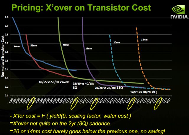
 Interesting article from Joel Hruska on ExtremeTech: Nvidia deeply unhappy with TSMC, claims 22nm essentially worthless . The title is a bit dramatic (poetic license) but the charts are accurate to the degree that 20nm costs will be significantly higher from the start and will continue to be higher throughout production and maturity.
One reason is double patterning, which is required at 20nm (double patterning splits a design into separate masks when devices are too close together). If 28nm masks cost $3M, 20nm masks will cost $5M or more. Another reason is design complexity: layout dependent effects (LDE) and process variation will get worse at 20nm, simulation and verification requirements will explode, and the list goes on…
Life in the semiconductor ecosystem certainly gets more complicated when you try and cram 30B+ planar transistors on one chip, absolutely!
There is no doubt in my mind that these slides are authentic. NVIDIA CEO Jen-Hsun is quite the showman and has a reputation for this kind of public grandstanding. I was a little surprised that NVIDIA used some sort of “normalized” $$$/transistor as a key metric, rather than more traditional semiconductor scaling measures, but perhaps that’s part of their internal business model.
One thing you must know, Jen-Hsun Huang and Morris Chang are VERY close, so you have to play a game of chess here and ask yourself what the agenda really is. A public whipping such as that? Openly criticizing your good friend and founding business partner?
Check out this video at the Silicon Valley Computer Museum, Jen-Hsun interviews Morris, it starts at 8:30 minutes in:
This video will give you a good understanding of the relationship between Jen-Hsun and Morris. It also provides a candid view of Jen-Hsun’s personality, which seems somewhat narcissistic to me.
This topic is certainly timely since the annual TSMC 2012 Technical Symposiumwill take place on April 17[SUP]th[/SUP] at the San Jose Convention Center. Trust me, you’re not going to want to miss this one!

Join the 18th annual TSMC Technology Symposium and get first-hand updates on TSMC’s advanced and specialty technologies, advanced backend capabilities and future development plans!!
- TSMC’s 20nm and 14nm process development status including FinFet and advanced lithography insights
- TSMC’s New High-Speed Computing, Mobile Communications, and Connectivity & Storage technology development
- TSMC’s robust Specialty Technology portfolio that includes Backside Illumination (BSI), Embedded Flash Power IC and MEMS
- TSMC’s new and exciting GIGAFAB™ new programs and improvements that enhance time-to-volume
- TSMC’s advanced backend technology for 3D-IC, CoWoS (Chip on Wafer on Substrate), and Bump on Trace (BOT)
To me this is a simple case of wafer pricing negotiations gone wild. Since TSMC is in such a dominant position at 28nm and 20nm the industry is telling them, in the Year of the Dragon, to be more like a teddy bear and collaborate on pricing in the same way they collaborate on technology.
But it’s ridiculous for any fabless semiconductor company to say that they will not aggressively transition to the coming process nodes (20nm and 14nm)! I remember back in the day buying an AMD 40MHZ based PC versus an Intel 36MHZ. Seriously, did I really need that extra 4MHZ? Did I pay extra for it? Of course!
At AMD’s Financial Analyst Day, CEO Rory Read made a point of saying that the company no longer intends to aggressively transition to new process nodes given the diminishing marginal returns from doing so.…….
Okay, let me clarify, any leading edge fabless semiconductor company that wants to STAY in business will aggressively transition to the coming semiconductor nodes, absolutely. Just my opinion of course.
Share this post via:


Comments
0 Replies to “NVIDIA Claims TSMC 20nm will not Scale?”
You must register or log in to view/post comments.