Introduction
At the recent Intel Architecture Day presentations, a breadth of roadmap plans were provided – an earlier article focused on the x86 client and data center cores and products. This article focuses on the GPU and IPU announcements.
Xe Graphics Core
The Intel GPU architecture for embedded, discrete, and data center acceleration is based on the Xe graphics core. The figure below illustrates the integration of multiple cores with other units to provide a “render slice” block in the overall GPU hierarchy.
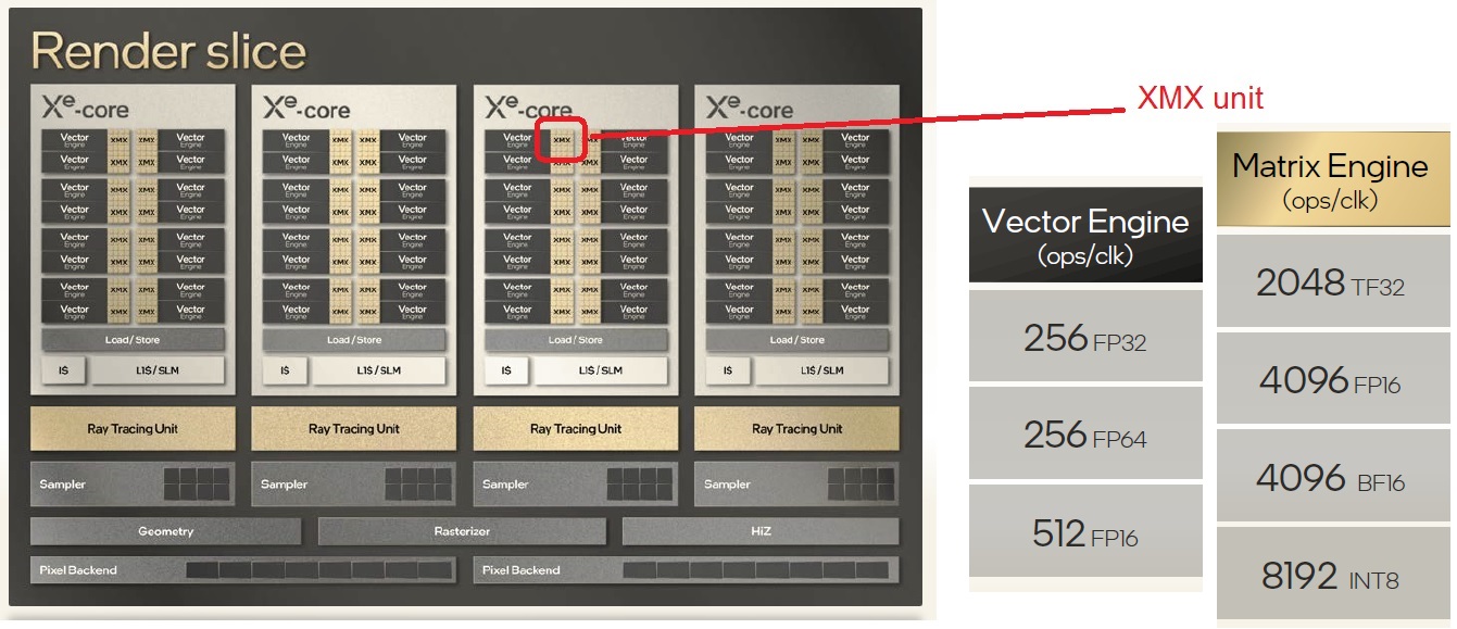
The Xe core supports both fp64/fp32 and fp16/bf16 data operands, to address both high-performance computing and AI workloads.
As was highlighted in the x86 core announcements, the integration of a “matrix engine” utilizes instructions and 2D data structures optimized for deep learning applications.
Arc
Intel introduced the Arc brand, to refer to the discrete graphics card product roadmap. Arc also incorporates new “unified, re-factored” graphics software drivers.
The first Arc card is codenamed “Alchemist”, with a Xe chip fabricated using TSMC’s N6 process (1Q2022).
XeSS Super Sampling
A unique software feature added to the GPU family is Xe super sampling. This image sampling method utilizes a combination of spatial and temporal data to upscale frame resolution, such as a 1080p to 4K video stream.

The graph on the right in the figure above illustrates the time to render an image for various methods (shorter is better). The XeSS algorithm combined with the XMX vector accelerator unit enables excellent 4K image throughput. Intel provided a demo of a 1080p video upscaled using XeSS to 4K resolution – the distinction between the upscaled and native 4K video (@60fps) was imperceptible, offering a unique power/performance optimization. (Intel indicated that XeSS was “neural-network driven”, but did not delve into detail.) The software development kit with XeSS support will be available shortly (for with hardware with and without XMX, utilizing the DP4a instruction).
Ponte Vecchio High Performance Computing GPU
The most advanced illustration of Intel’s packaging technology was provided as part of the Ponte Vecchio data center GPU presentation.
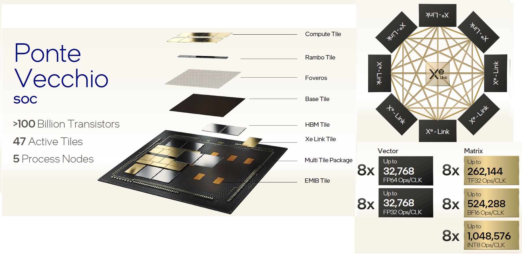
The (massive) package integrates various tiles, and utilizes both Intel’s 2.5D EMIB interconnect bridges and 3D Foveros vertical stacked die. Of particular note is the constituent tiles are sourced from both TSMC (e.g., compute tile: TSMC N5) and Intel (e.g., base tile: Intel 7).
The Xe link tile (TSMC N7) enables direct connection of a variety of GPU topologies, as shown below.
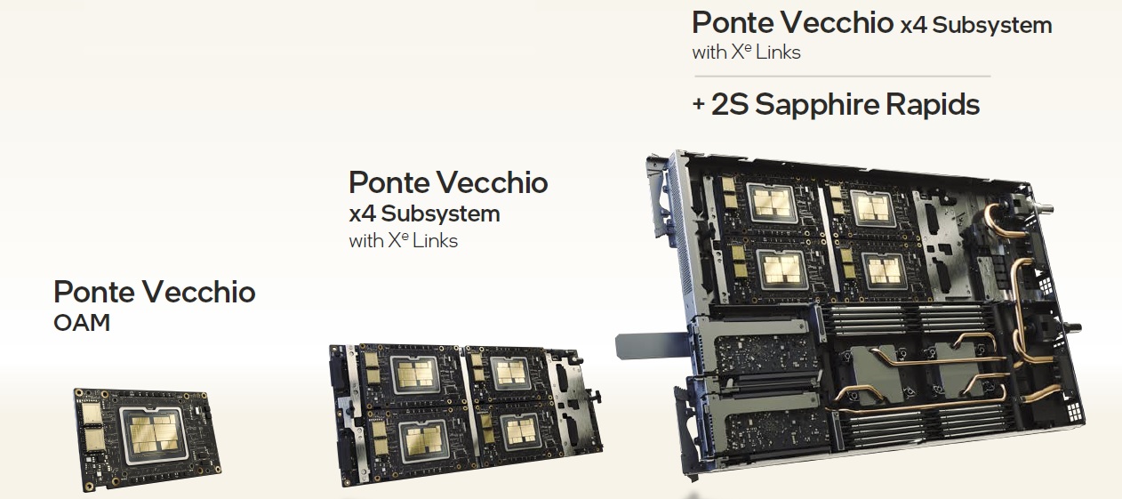
Preliminary (A0 silicon) performance measurements indicated an extremely competitive positioning relative to the GPUs in prevalent use in today’s data centers.
Infrastructure Processing Unit (IPU)
Intel provided a very compelling picture of the inefficiencies in current cloud data center services. The figure below shows that a “traditional” CPU plus SmartNIC cloud server architecture requires that the CPU spends considerable cycles performing infrastructure micro-services, such as storage management, security authentication, data encryption/decryption – a range of 31% to 83% overhead, as illustrated below.
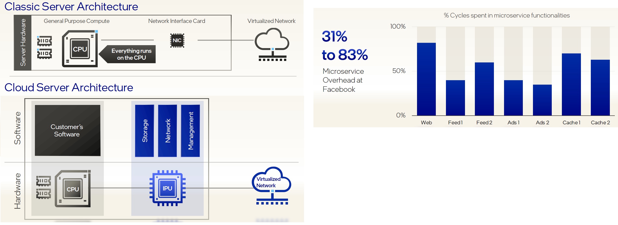
These cycles are non-billable from the cloud services provider (CSP) to the client running “tenant code”, a considerable loss of revenue for the (expensive) CPUs in the data center.
Intel indicated they have been working closely with a “major CSP” on the design of an Infrastructure Processing Unit (IPU), to offload the CPU from these tasks and thus, increase cloud-based revenue. (SmartNIC cards help accelerate some infrastructure tasks, but are a peripheral device under the control of the CPU. The IPU offloads infrastructure functions and offers an additional layer of security and greater flexibility in host-to-storage configurations, by separating tenant tasks on the CPU and CSP infrastructure functions on the IPU.)
Intel showed both an FPGA-based solution, and a new ASIC-based IPU named Mount Evans, as shown below. The cores in Mount Evans are based on the new Arm Neoverse (N1) architecture that is tightly coupled with the best-in-class packet processing pipeline and hardware accelerators.

OneAPI
Briefly, Intel described their work on the industry-standard “OneAPI” software toolkit development, an effort to provide:
- a data-parallel software language (e.g., DPC++, especially for accelerators)
- an open S/W development stack for CPUs and XPUs (e.g., GPUs, accelerators)
- software library APIs for machine learning, video/media stream processing, matrix/vector math
- a full development toolkit (compiler, debugger, accelerator hardware interface models)
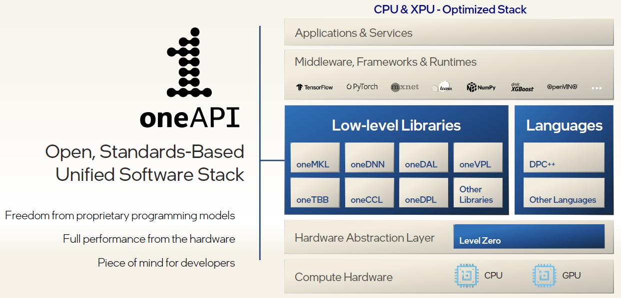
Key areas of focus are the:
- the definition of required hardware accelerator capabilities and services to interface with the software libraries
- acceleration of data de/compression
- optimization of the map-reduce framework (for faster database searches)
- optimization of the data storage footprint
For more information on OneAPI, please refer to: www.oneapi.com .
Summary
Although best known for their CPU offerings, Intel’s breadth encompasses a much richer set of computing hardware and software products. At the recent Intel Architecture Day, they presented an aggressive roadmap for integrated, discrete, and (especially) data center GPUs, vying for leading performance across the full range of enthusiast/gamer and data center applications.
A close collaboration with a major CSP promises to significantly upgrade the efficiency of cloud operations, replacing the SmartNIC with a richer set of functionality in the IPU.
The OneAPI initiative will no doubt lead to higher software development productivity across a myriad of CPU plus accelerator architectures.
The Ponte Vecchio GPU deserves special mention, as an example of the tradeoff decisions in building a complex GPU accelerator, integrating silicon tiles from both TSMC and Intel foundries with Intel’s advanced packaging capabilities.
-chipguy
Share this post via:


Comments
There are no comments yet.
You must register or log in to view/post comments.